The NED Synclavier is an awful combination – complex circuitry built up of hundreds of (mostly TTL) ICs and no documentation in the wild.
So there’s no way around getting intimate with circuitry to understand how things work to make my latest project possible. First of all I needed an idea how everything is timed – a most important point in a serially operating system. Similar to the Able processor itself, the Sample-to-Memory unit makes use of an unidirectional 16 bit parallel bus on which control information, memory addresses and finally data are sequentially transfered.
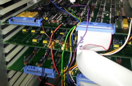
All information propagate through the daisy-chained modules PSF, PSADC, PS(B)MC, DDDAC and then back to PSF, while the four timing signals into which all communication is framed traverse the chain in the opposite direction. To learn how this actually works, I’ve hooked up a minimal memory chain setup consisting of only the PSF and a PSMC. As the PSF gets the actual timing from the PSSRGA, the latter board is also installed in the poly bin:
The analyzer probes bring some color into the bin.
It was a quite succesful session so far, the bus timing is no secret to me anymore.
Stay tuned for the next steps on a long way…

