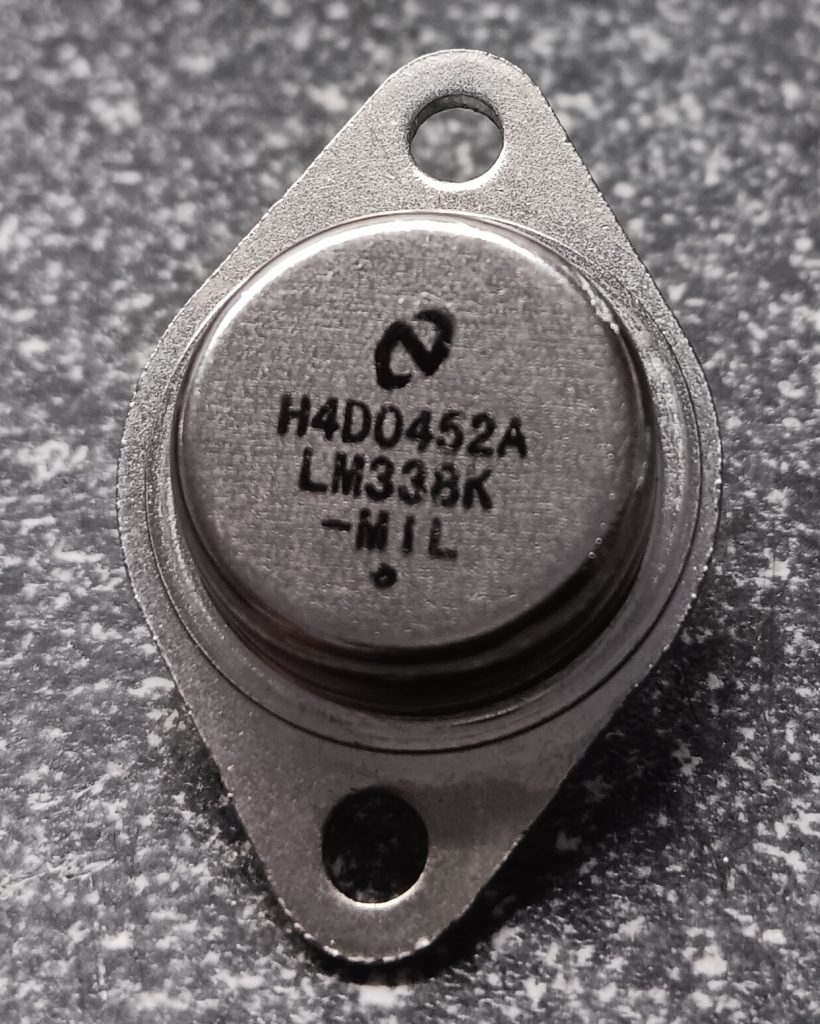
As the adjustable 5A regulator LM338K is usually sold for around 100 currency units, anything well below this figure will very likely be a counterfeit part. I got some with a troubleshooting job and could not resist to check them.
While the printing already looks fishy, it seems to be what it claims to be, it behaves like any LM317/350/338 type regulator under low load. But when increasing the load, it quickly became clear that it is not a 338 as the current remained well below 2A and then suddenly dropped to zero.
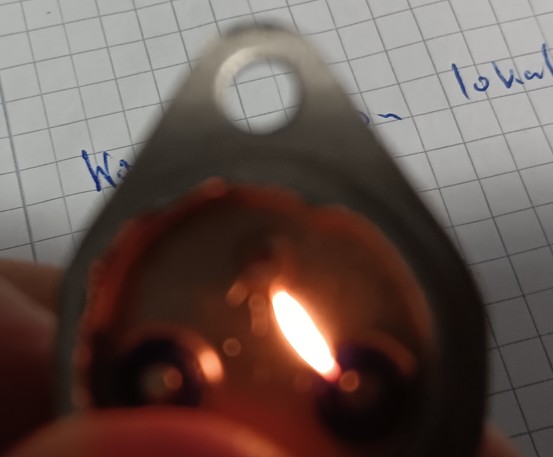
So I opened up another specimen and had a quick look through a microscope – the die clearly says 317 (no photo made, sorry). But it does not even fullfil LM317K specs, here is the opened device running at around 0.9A
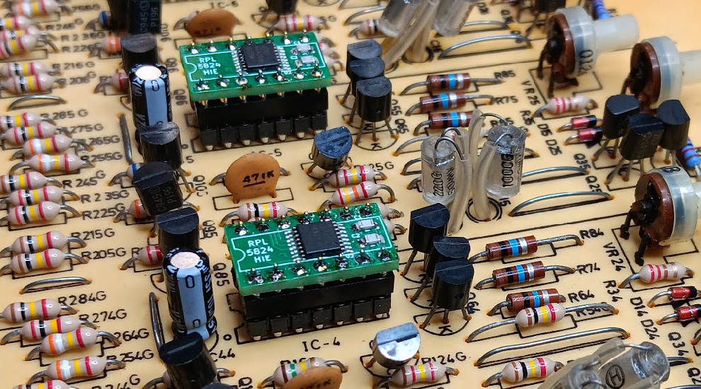
There are various approaches for replacing the MM5824 divider chip, prominently used in KORG PS3x00 series synthesizers.
Most are based on the replacement circuit KORG themselves used on their boards. It consisted of a Hitachi HD14520 and some passive components. Many replacements just use a competitor’s 4520 type counter IC and maybe adjust the values of the passive components.
What I encountered when using such replacements: when holding certain notes, the tone eventually became interrupted at random intervalls. The counters occasionally counted mutiplie times during one cycle of the input signal due to violation of the input slope. The original HD14520 allows for 15µs rise and fall time for all supply voltages between 5 and 15 volts, while for example TI allows 15µs at 5V but only 5µs at 10 or 15V VDD, and Nexperia calls for 3.75µs@5V, 5µs@10V and 9µs@15V.
The obvious solution to get rid of any manufacturer constraints was to add a Schmitt Trigger to the circuit, which I did for both clock inputs while keeping attention to the clock edge on which the original counter propagates.
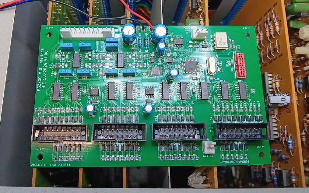
Here I want to introduce my approach to MIDIfication of the KORG PS3x00 series. It is not really different from previous solutions, but for me it has the advantage of being available when I need one.
The features: – MIDI In only – drives the 49 key contacts with the full voltage swing – allows for program change in the PS3200 synthesizer – has 8 1/4″ outputs, routed to an external breakout box featuring also the MIDI connector and a “learn” button to set parameters – 6 of the analog outputs can be unipolar (0..+5V) or bipolar (-5..+5V) or a simple 0/+5V switching function and assigned to any MIDI CC – 1 output is mapped to pitch bend with 14 bits of resolution – 1 output is mapped to modulation
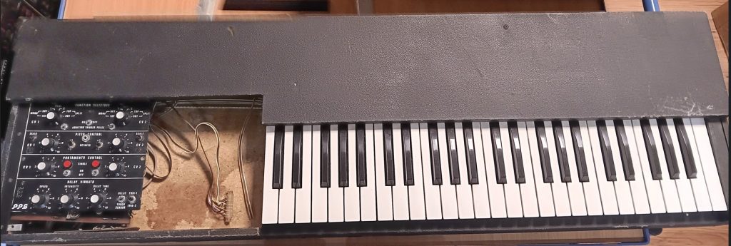
The PPG digital keyboards were a completely new approach in controlling analog modular synthesizers. While most other manufacturers(*) used resistor strings, sample&hold circuits and eventually means of analog computation to achieve polyphony, Wolfgang Palm of PPG went the digital way. This allows for completely new voice assignment schemes and complete pitch stability after a key is released.
The references I found vary a bit in functionality. A Duophonic Keyboard 322 I found on the web for example has one switch setting for monophony, duophony, split mode and a button-activated memory mode, which is also described in the “INFO MAPPE SYNTHESIZER MODUL SYSTEM 300er SERIE” from December 1976. Also in this publication there’s a photo of a multicontrol keyboard similar to the one described in this post.
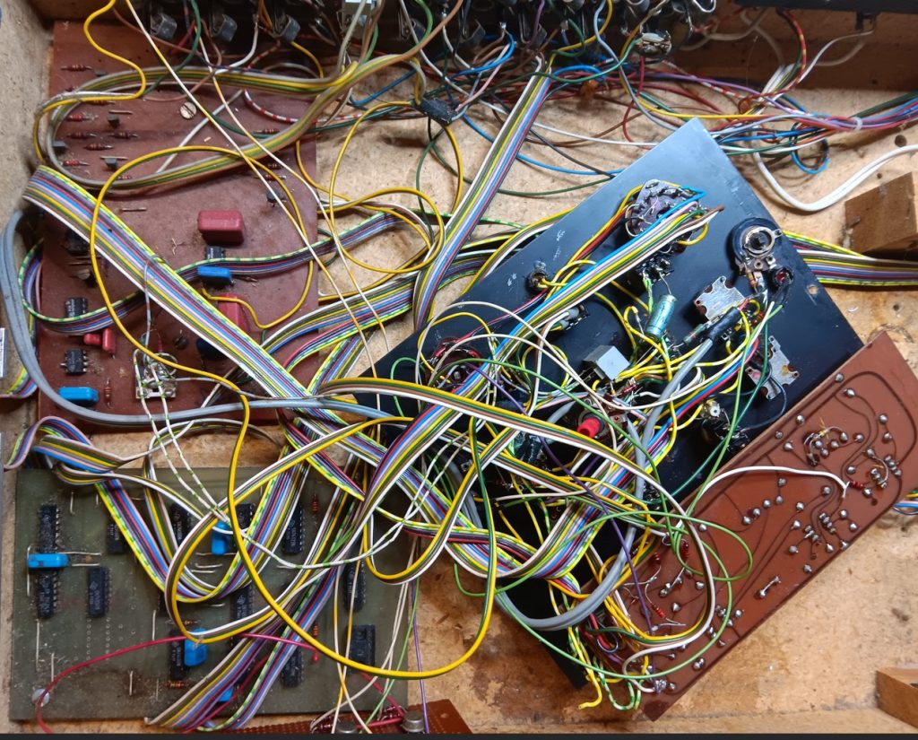
It came to me in parts, with lots of the internal wiring cut and rewired for some unknown purpose. The goal is to restore full original function, while adding the previously removed internal power supply, and to reverse engineer all of its circuitry to create some documentation also for its usage from this.
(*) Oberheim used a digitally scanned keyboard around the same time in the FVS, but there are probably not many more examples.
Before I start over with individual posts showing the functional units of the keyboard, here is a first impression of how it came to me and how important a careful disassembly, documentation and restoration will be.
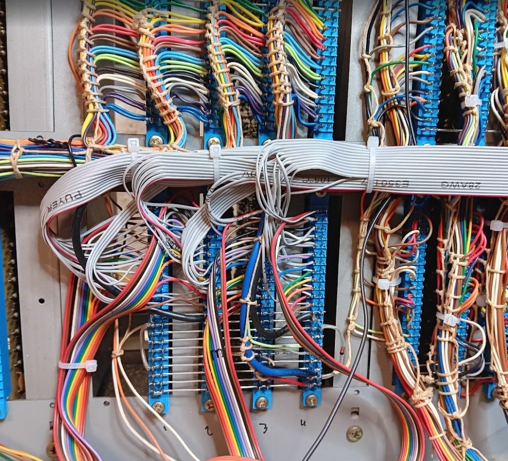
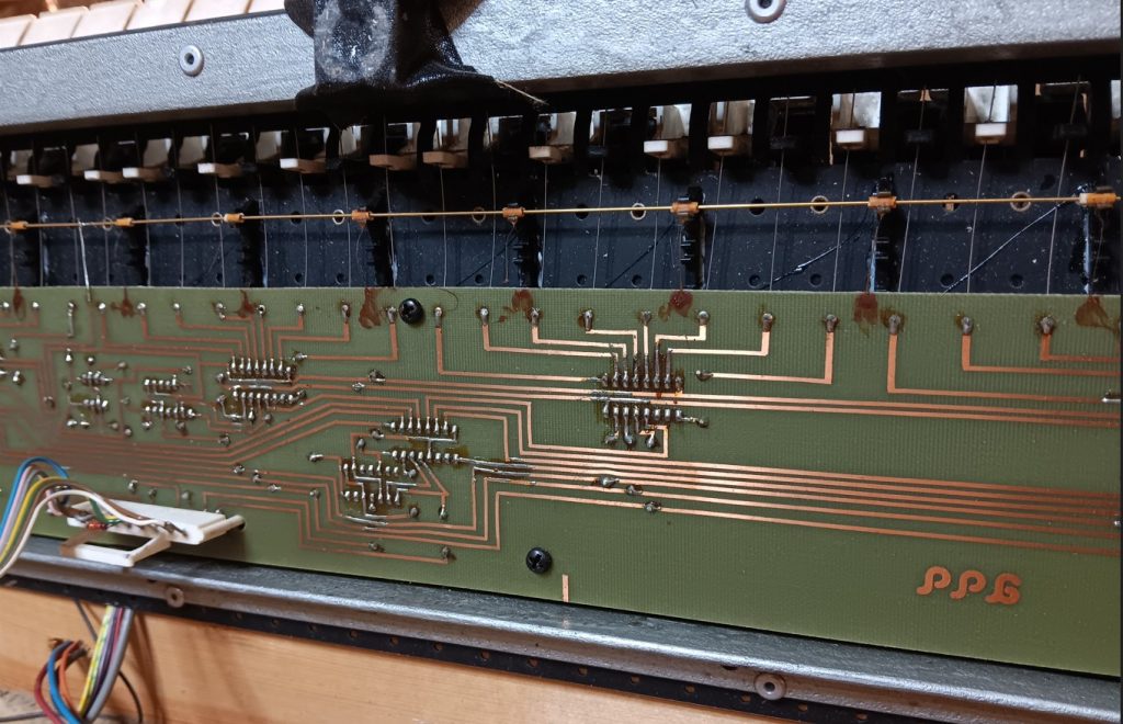
The keyboard is based on a rather typical J-wire style keyboard. 49 J-wires are sequentially pulled to ground by means of a counter/decoder circuit on the keyboard assembly itself. This is synchronized by several signal lines with the keyboard assigner circuit on one PCB below the left hand control panel.
Circuit description
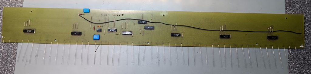
For all circuit descriptions I will use my redrawn schematics attached to the post. The part designators are randomly chosen as none of the original PCBs has component designators of any kind.
The whole scanning of the keyboard including the storing and assigning of key data is clocked by a 555 timer IC running at 14.6kHz with an almost symmetric output. This clock is fed to the assigner circuit by the grey wire connected to pin 6 of the multi-pin connector. Simultaneously it clocks a cascade of two SN7493 4-bit counters. They are arranged that 6 outputs define 64 time slots of 68.5µs, so a whole scan cycle takes 4.4ms. The lower three bit are connected to the ABC inputs of 7 SN7445 BCD decoders, while the upper three drive another SN7445 which in turn enables one out of the 7 other 7445. As the Q0 output of the latter 7445 is unused, the actual keys are mapped to the time slots 8 to 56. The last decoder output, which goes low in the 63rd time slot and is used for synchronization purposes via the blue wire on pin 9 of the connector. Additional timing information is derived from the 6th bit of the counters (U3 pin 8) which, via the white wire on pin 1, indicates whether the lower (key 1-24) or higher (key 25-49) half of the keyboard is currently scanned. This is obviously necessary to allow for split assignment. U3 pin 11, the 7th bit which is not used for the keyboard itself, is also sent via pin 2, brown wire, to the assigner circuit. This plays an important role in the control circuit for the key memories as the actual key data is only interpreted in every other scan cycle, so the real scan time becomes 8.8ms rather than the previously mentioned 4.4ms. The pink wire on pin 7 carries the actual key data, it becomes low for every timeslot in which the associated key is pressed.
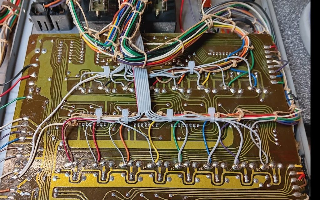
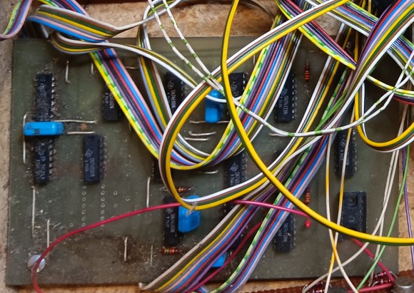
The key assigner allows to generate two independent control voltages and gate signals from the time multiplexed data from the keyboard circuit. Each output can be selected between two monophonic, two duophonic and two key-split modes with a fixed split point between key 24 and 25 (see above).
To achieve this, the pulse train from the keyboard is stored in two 64 bit serial shift registers (Texas Instruments TMS3417). Those are controlled using the synchronization signals from the keyboard circuit, the mode switches on the front panel and a circuit defining whether the real time keyboard data or the recirculated output is fed into the registers. The shit register output, together with additional control signals, are fed to a second PCB which converts the pulses (not parallel digital data!) to the precise control voltages.
Seit dem ersten Umbau sind einige weitere Willies zu mir gekommen. Auch in der Variante mit Uhr und dem liegenden Willie auf der Bank konnte ich die bestehende Platine verwenden, sie wird hier lediglich um 90° gedreht eingebaut.
Für das Lautstärke-Potentiometer habe ich nun eine einheitliche Lösung (Foto fehlt noch), bestehend aus einem Piher PT10MV Trimmpoti (Sechskantantrieb) und der passenden Steckachse. Durch die höhere Bauform muss die Platine mit zwei 3mm Distanzstücken und entsprechend längeren Schrauben montiert werden.
Aktuell ist eine Platine für die Willie-Varianten ohne Uhr in Arbeit. Bei der stehenden Figur würde zwar die vorhandene Platine passen, der Halter für die Platine nimmt aber nur die kleinere Version auf, so dass ich eine direkt passende Variante ohne Eingang für den Uhrenkontakt entworfen habe.
Die üblichen Verschleißteile fallen bei allen Modellen an, als da wären die Batteriekontakte (hier verwende ich Typen von Keystone, die mit kleinerer Anpassung an Kontakt und/oder Kunststoff-Bodenplatte sicher eingebaut werden können, sowie ide Gummiriemen. Aktuell verwende ich vom Durchmesser passende Vierkantriemen mit 1x1mm, die etwas höhere Reibung verglichen mit den 0,75mm/0,8mm Riemen des Originals scheint kein Problem darzustellen, allerdings baue ich normalerweise auch die Andruckrolle für das Tonband aus.
Recently a half repaired OB-Xa hit the workshop. The main trouble was complete failure to auto tune. After fixing some obvious faults (damaged vias, poor quality trimpots) the auto tune issue remained. Although the serial number indicated “old” auto-tune the program LED advanced during auto tune, so the firmware has been upgraded to a revision C already.
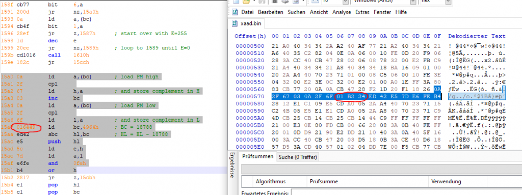
Until now I have always ignored that the service manual does say that the Revision C software has a new auto-tune circuit – so I had to learn it the hard way. I measured the gate time of the period meter circuit (which is around 3.82ms for a well tuned VCO, 4 periodes of a high C at 1046,5Hz), measured the clock frequency which is half the crystal clock or 2.4576 MHz. This gives a period count of around 9400.
Now I disassembled the firmware and saw that the target count is not in the 9400 range, but twice of that – 18,788 ! I verified my assumptions by feeding a 523Hz clock from a DDS generator which instantly let auto-tune pass.
During this, I also used the great “XACA2” patch EPROM from Ricard Wanderlöf (read here http://butoba.net/homepage/synthhacks.html). We had an email chat for some days trying to evaluate what is happening and came to the conclusion that all out assumptions must be right and that there must be a hardware change as well.
But first my comparison between the XAAD firmware (the last of Revision A) and the XACA disassembly:
While the Revision C compares the period count with 18,788, the old revisions indeed had a target value half as high!
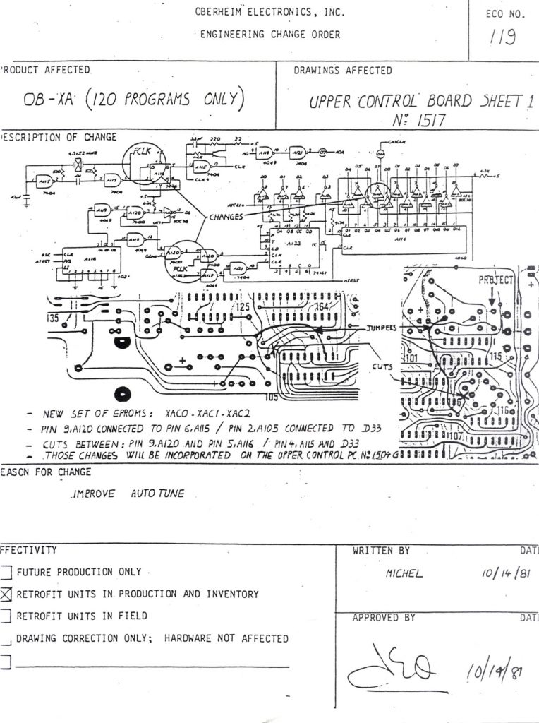
So the only solution to this can be that the period meter is clocked from the full crystal frequency of 4.9152 MHz for Revision C and higher. Half an hour(!) I made this conclusion I found the ECO #119 which explained how to change the upper board for use with the Revision C firmware.
Some times we learn it the hard way. Lots of techs I asked during the process weren’t aware of the hardware modification – or just forgot about it, 40 years later…
Interesting enough: the original schematics of the later mainboard type for the Revision F and G firmware still show the period meter clocked by 2.4576MHz, while the target value in the firmware remains at 18,788. So this must be an error in the diagram, probably not the only one.
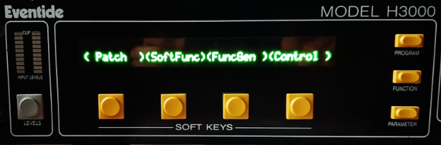
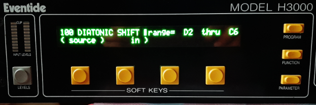
The H3000 is one of the examples that shows us that common OLED displays claiming to be HD44780 compatible are not, in several aspects.
We have three faults here:
missing first line in most of the Soft Functions pages, caused by the fact that a Clear command (0x01) does not “home” the cursor, although the WS-0010 datasheet (the most common OLED controller) says it does
stuck text “in ]” above Soft Key 2 that results from the firmware copying screens by reading the DDRAM and writing it back when needed, using the auto-increment function of the controller which behaves differently between HD44780 and WS0010
wrong characters (Japanese symbols) due to the OLED having four character sets, with the needed not being default
While changing the character set is as easy as using 0x39 instead of 0x38 for the standard LCD init sequence, selecting the western european charset, the first fault already required a small subroutine that homes the cursor after clearing the screen.
I did not even try to shift around code in the EPROM to obtain the space needed for the additional home command because the disassembly gives hints that certain routines are called from without the main firmware. Instead, I modified the chip selection by fitting a larger PLD instead of the PAL16L8 used for address decoding. This way I was able to use the 256 bytes of unused space at 0x8200 for my own routines.
This was necessary especially as the second problem, the stuck text, required to replace the routines that read and write, respectively, the screen from/to the DDRAM by new code that initially reads the current internal address of the display, keeps track of it while the display is read or written, and inserts a command to re-position the cursor when the pointer would normally wrap around into the second line on a standard HD44780 display.
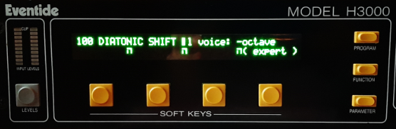
Finally, a working OLED in a H3000 (with H3500 firmware)
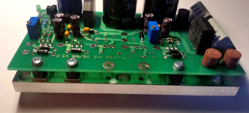
The SCI Prohet 5 Synthesizer has thermal issues in the power supply. SCI’s attempt to make do with a single CT secondary winding results in a voltage of up to 25VDC before the 7805 series regulator. The lack of a decent heatsink makes this even worse. Several techs have been rebuilding the stock PSU with either an additional tranformer or by replacing the transformer with a new one with an additional winding, supplying around 9 volts to an additional rectifier.
This modification also requires some work on the reset circuitry, otherwise the RAM contents might be damaged on shutdown. Other typical work covers replacing the thermal interface material, the big filter capacitors and the tantalum capacitors on the PSU board.
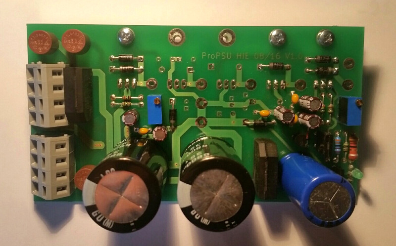
I decided to somewhat standardize the PSU maintenance of Prophet 5’s by designing a drop-in replacement PSU board I called the ProPSU. In order not have to temper with the name plate I made a aluminium heat spreader that is tightened to the back (use of some thermal compound is highly advised!) by re-using three of the original screws. The ProPSU board itself will be, after the cable harness is soldered to the ProPSU, bolted to the readily attached heat spreader by means of 3 or 5 M3x16 machine screws.
The ProPSU can be used for both Rev.2 and Rev.3 Prophet 5’s, with either the +12/-5 volts rails for the 2708 EPROMs provided or missing. Both 15V supplies can be adjusted by means of multi-turn presets. An on-board reset circuit switches the “+20V” rail to the mainboard’s reset generator, simulating a quickly discharging filter cap when the +5V supply drops below 4.75 volts. On turn on, the delay of the reset circuit ensures that all voltages are stable.
Ready to use ProPSU for late Rev.3 or modified Prophet 5 (new EPROMs, no +12/-5V required)
Mounting detail: the heat spreader bar is attached to the bolts of the old PSU’s regulators, after that the ProPSU
PCB is mounted to the heat spreader (isolation washers not shown here)