As circuit design is finished and most PCBs are populated now, it’s time for assembly.
First of all the controller boards need a place:
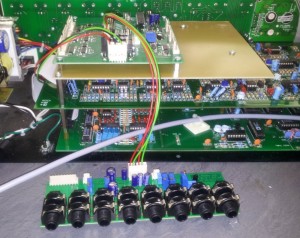
Here you can see the Controller Board on top of the original SE1X CPU and analog boards.
An additional copper-cladded PCB should prevent digital noise from the new microcontroller to disturb the analog board, although the small ATmega @1MHz with no fast clocked outputs would not make much EMC trouble either. The Controller Board gets its +/-15 volts supply directly from the PSU, all other voltages (+/-12, +/-7, +5) are generated on board.
The board lying on the table is one of three VCO jack boards. The functions of its 8 jacks is alrady outlined in the previous post.
I thikn it’s time to wire & fire things up…
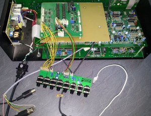
The MIDI jacks from the SE1 CPU board have been removed and extended by shielded cable to allow the DIN jacks to be fitted in the new rear panel, same will apply to the IEC power connector.
Yes, it’s supplied from an isolation transformer, and yes, the open frame PSU is a nasty little devil and will be replaced by something more safe and silent.
The VCO1 Jack Board is now connected to the Controller Board by several (yellow) cables, carrying control voltages of different kind. The two shielded cables are hooked up to the analog board – one in between the VCO output and VCO Amount VCA input, the other one delivers the triangle output to the sine converter on the Jack Board. The sine wave is mixed to the VCO output under control of the Controller Board, eventually overriding the command from the SE1 CPU.
On the photo above I was adjusting the Middlebrook & Richer triangle to sine converter that any of the 3 VCO Jack Boards features to allow all three VCOs producing sine waves. I was quite surprised that I got the 2nd harmonic down to -50dB and the 3rd to -40dB, measured at 440Hz. Overall THD will be in the 1.5% range, maybe even better when final adjustment are made.


