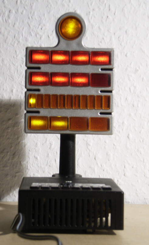
Berlin Clock

berlinuhrThe “Berlin Clock”

also called “set theory clock” or “Mengenlehre-Uhr” in German.
The time is displayed by the count of illuminated fields, weighted by their value:
– lower row: 0 to 4 fields indicating 0 to 4 minutes PLUS
– 2nd row: 0 to 11 fields indicating (0..11) * 5 minutes = 0 to 55 minutes PLUS
– 3rd row: 0 to 4 fields indicating 0 to 4 hours PLUS
– upper row: 0 to 4 fields indicating (0..4) * 5 hours = 0 to 20 hours

The round field on top is illuminated for every other second. Additional, small LEDs in the top field show whether an alarm is set and activated.

The time shown on the photo?
4*5h + 3*1h + 1*5m + 2*1m = 23:07


History


The Berlin Clock was designed by Dieter Binninger in 1975. Some information can be found on Wikipedia: https://en.wikipedia.org/wiki/Mengenlehreuhr
Small table top models were sold by souvenir shops in the 1980s, as well as a wall clock. All of those suffer from the amount of heat generated by the transformer(s) – 1 for the table version, 3  for the wall clock – which makes the plastic brittle. To save or restore a Berlin Clock, it is highly advised to remove the transformer and use a wall-wart type power supply which is easily possible with the circuit introduced below. It can even recover a clock with a defective processor, which was a 4 bit controller with mask ROM made by Texas Instruments.
While the table version already used LEDs, the wall clock had miniature incandescent lamps, therefore the need of three transformers. I have modified a wall clock by installing high efficiency TOPLEDs in place of the lamps, effectively eliminating two of the three transformers and reducing the heat.

The Circuit


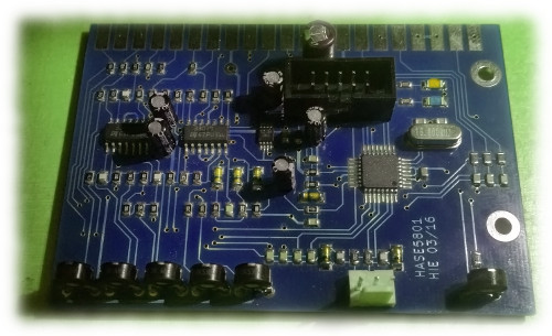
My circuit replaces the custom micro controller, the LED driver ICs and the whole power supply circuit board. I used an Atmel ATmega8 CPU which drives the LEDs by discrete PNP transistors for the high side and a ULN2003 array for the low side. The LED circuit board can remain in the original state; the 14 way DIP connector fits directly in the socket on the replacement board. I recommend to replace the old, not very efficient LEDs by modern high-efficiency types though. As for the original, the time base is derived from the mains frequency. Therefore the current firmware requires the clock to be run from a 50 Hz mains with a high long-time precision. The circuit board with the processor and driver ICs carries the contacts of the push buttons as well, so I suggest to remove all parts but the diodes shown in the photo below from the board and re-use it. 6 wires need to be soldered to the locations of the processor’s place as indicated in the circuit diagram.

berlinuhr_cabling


Emptied original PCB with the 6 wires for the switch matrix attached. 3 diodes and 1 jumper wire remain in place, the other components need to be removed.

berlinuhr_inside

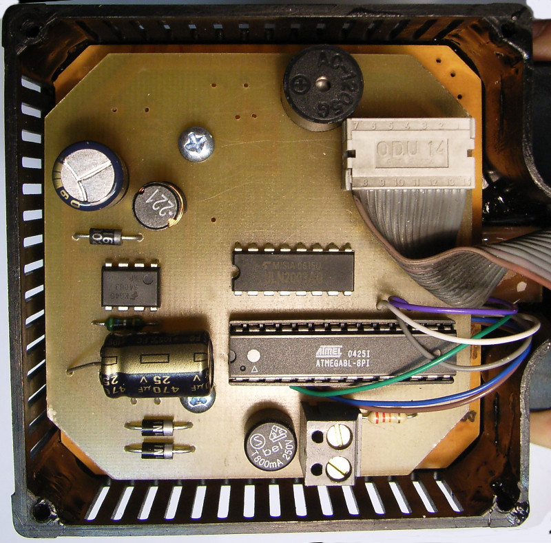
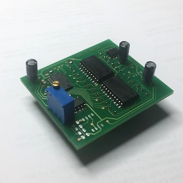
Replacement circuit fitted to the clock case. The 14 way connector from the LED board fits to the socket on the PCB. The screw terminal on the bottom connects to an AC wall-wart type power supply delivering 12v AC, current consumption is well below 200mA thanks to the used switching regulator which provides the 5 volts for the micro controller and LEDs. The speaker on top is a dynamic loudspeaker, no piezo, and without integrated electronics, with a DC resistance of about 50 ohms.

berlinuhr_pcb_solder

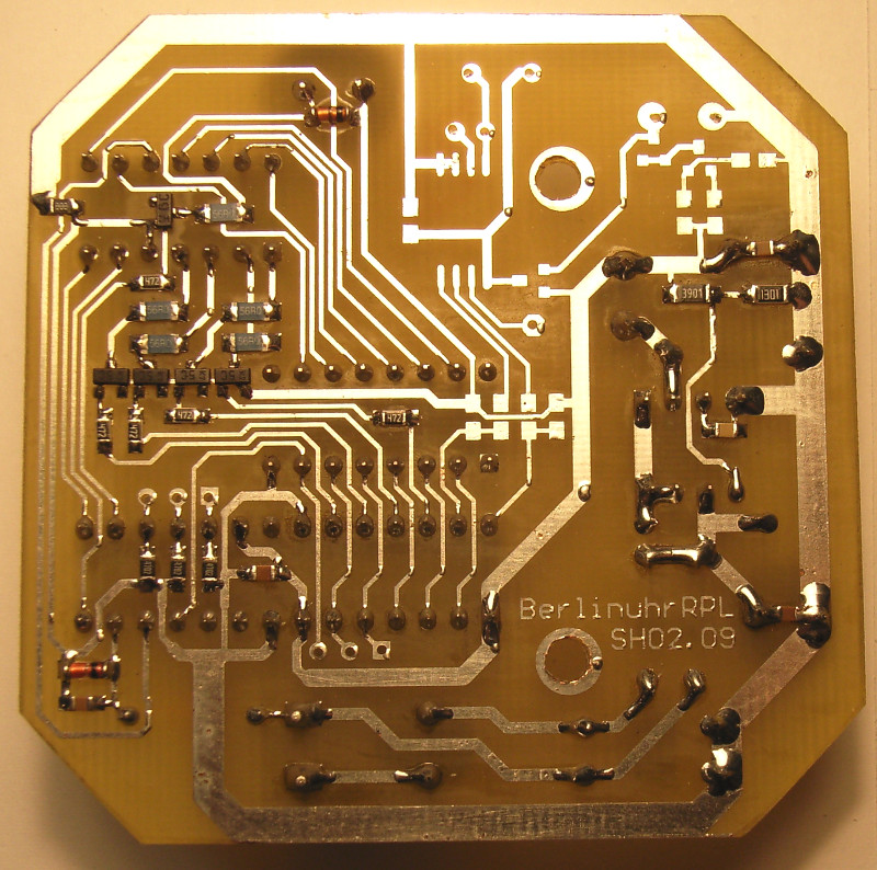
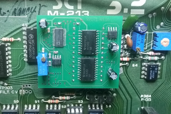
Solder side view – some SMD components are in use, capacitors and small resistors are size 0805, the resistors above the MC34063 on the right and the 4 56ohms resistors for the LEDs are size 1206. The unpopulated locations are reserves for a PCF8583 I²C real time clock circuit which would make the Berlin Clock independent from line frequency and preserve the time during mains outage. This function is not yet implemented in the current firmware. If anyone feels free to add it, please ask for the C code (WinAVR/AVR-GCC).

Firmware


The software is written in C (AVR-GCC). As written above, the current version uses the mains frequency of 50Hz as a timebase and makes no use of the RTC chip provided on the PCB layout. All functions of the clock have been programmed to resemble the original behaviour. The wrap-around at midnight works exactly as in the original: 23:59 -> 24:00 -> 00:01.

Downloads


This project is free under the terms of the Creative Commons by-nc-sa licence (use and alter it for non-commercial purposes provided my name remains in the work).
The files needed to produce the PCB, build the circuit and program the micro controller can be downloaded here:

berlinuhr_schematic PDF file of the schematic diagram

berlinuhr_pcb PDF file of the PCB layout (size 100% when printed on A4)

berlinuhr_cam ZIP archive of CAM files (Gerber for solder side copper and solder mask plus drill file) for industrial PCB production

berlinuhr_firmware ZIP archive with hex file for programming the Atmel ATmega8 micro controller.
Make sure you set (write a “0”) the following fuse bits when programming: SUT0, CKSEL2, CKSEL3 and BODEN. All others should be unset (remain “1”).

APR Odyssey: CV/Gate for the White Face

Several approaches of adding CV/Gate to the Mk I Odyssey consist of not more than 3 or 4 1/8″ jacks with switch contact that interrupt and hook into the internal CV, gate and trigger lines. While the CV uses standard 1V/octave, the gate and trigger signals require a rather high amplitude of about 10 volts, with the additional impact that the gate level has a direct influence of the achievable output level of the AR envelope. Furthermore, both gate and trigger signals are needed for most modifications.

By adding a simple transistor circuit that resembles the levels generated by the Odyssey’s A board this ARP now works perfectly even with 5V gate and trigger levels and does not require the separate trigger signal anymore, although the trigger input jack is still provided for special purposes.

Odyssey Gate CV

The prototype for the improved CV / Gate modification in action


PPG 390 Drum Unit

One of the most rare PPG units found its way to my workshop recently: the 390 Drum Unit.
PPG 390 Drum Unit

Basically, this is a very rudimentary 8 bit sample player. It features 8 drum sounds in EPROMs on 4 voice cards. Two clock sources drive the address counters on the boards, which means that Sample Freq 1 defines the sampling rate of the odd channels, while Sample Freq 2 is in duty for the even numbered instruments.
[Block diagram to follow…]

Upon arrival one card was missing, instead I found a non working wire-wrapped vero board with a prototype for a single 4kByte instrument in two 2716s, and two 2732 EPROMs with instruments samples that won’t fit anywhere. I designed a PCB to replace the missing voice card, providing sockets for 2764 EPROMs so experimenting with other samples woule be easier as they can be programmes with cheap USB programmers.

PPG 390 Voice Card

Once completed the design I realized that I cloned the original cards so perfectly that I still don’t have a use for the 2732s – but my layout provides an easy solution, with two piggy-packed 4040 counters and some wires I modified my new voice card to work with the Noise and Hi-Hat EPROMs. Some more wires would allow to experiment with 2764 or even bigger EPROMs.

The clock frequencies are in the range of 13 to 30kHz, so the sound duration is between 70 and 160ms for the originally used 2716 EPROMs and 140 to 320ms for the 2732 sounds and would scale accordingly when using a larger EPROM.

PPG 390 Overview

Apart from this addition, the cards got guides (the blue things) to protect the connectors, new capacitors, additional capacitors in the output lines (originally it had a 3V DC offset), a new transformer, IEC mains jack, a mains fuse and a mains wiring according to current standards.

It is probably not an impressive drum unit sound-wise, but an interesting collectors item and I somewhat like the shaker … 😉

Posted in PPG

Advancing the Synthex

Four years ago I wrote “except the LFO section, because it’s strictly analogue”, but this did not really let me rest. So I started designing a new LFO board with some special features that can be controlled by the new processor board that is currently in development.

While the processor board design is near completion, a first prototype of the Advanced LFO has just entered the programming phase. Here’s a peek for those who are following the project for some time now. It’s alive!

Advanced LFO Board

RPL71 – Replacement for DAC71 series D/A converters

As stocks of working DAC71 series converters are depleted I designed a plug-in replacement for both the current (I suffix) and voltage (V suffix) types, including both CSB and COB coding. While the code is selected by a solder jumper, the voltage type replacement needs an additional SO8 OP Amp, like an OP07, fitted. The “TRIM” pin is not connected, instead of this a 20-turns potentiometer is added to the RPL71 board allowing fine adjustment of the on-board 10,00V reference. Where needed, a buffered output of the reference can be provided by adding another OP Amp and a few resistors.

rpl71_1

Shown above is a DAC71-CSB-I replacement board (no I-to-V OP Amp on the upper right side) and without a reference outputs (missing parts on the lower corner) which is equipped with a 14- instead of a 16-bit DAC to save 10€ as this board is tailored for use in Sequential Circuits Prophet-5 synthesizers where the lower 2 bits are not used anyway. The actual use case is shown below.

rpl71_2


Variophon: Electrical safety – naaah…

The Realton Variophon, a quite rare electronic wind instrument, is a frightening example how ignorant engineers can be when it comes to safety. While the whole circuit is a very interesting design and far from amateurish, the power supply is a completely no-go. To illustrate what I’m writing about, here’s a photo of the amplifier PCB that carries the mains fuse and switch connections:

  •  mains input is a standard IEC jack with the PE left unconnected, although exposed metal parts are present, but no proper isolation
  • the mains wiring are – 2 AWG28 litz wires from the IEC jack to the board above and 2 AWG 28 wires back to the mains transformer
  • those AWG28 wires are part of a 20 conductor flat cable, entering the PCB in the photo via pins 19 and 20 of the header
  • the track passing the mounting screw, that is actually in direct contact with the metal front plate, is isolated with a small nylon washer
  • the first and only fuse can be seen after the mains switch
  • next to the 4 header pins carrying 230VAC are secondary circuits which are in direct contact with the metal parts of the instrument

The only valid bet would be what happens first – electric shock or fire. This one obviously needs a serious rework.


PPG 1020: Digital keyboard?

The PPG 1020 is known as the stable successor of the 1002 synthesizer. This was achieved by use of a special oscillator architecture that combines digital octave division and a closed-loop approach including a VCO. The VCO covers the whole range(4 keyboard octaves + approx one more for the “digital modulation” feature), but being within a closed loop, it is stabilized to some degree. The details will be topic of a later blog post. For now we only need to know that we need a digital word that determines the octave and a control voltage to drive the VCO to one out of 12 semitones.

Even without the use of a processor (the 1020 does not have a computer of any kind) it would be straight forward: scan the 49 keys, somehow divide the number of the pressed key modulo 12, the result will be the (already digital) octave number, the remainder drives a DAC to generate the CV.

This “somehow” was actually done by using synchronously counting registers – a chain of 2 binary counters, one turning over at 12, the other incrementing whenever the first one turns over, and a chain of shift registers scanning the keys. The first “high” (pressed key) in the serial pulse train from the shift registers will latch the counter outputs in the next cycle, so we have a low-note priority here.

The counters mentioned above drive the octave control word and a digital-to-analog converter built from two 4051 multiplexers and a chain of accordingly weighted resistors. The reference voltage to that chain is generated on the main board and derived from the setting of the tune knob and the pitch bend slider.

For modulation purposes, an offset is digitally imposed. Since the modulation source from the main board is an analog control voltage, analog-to-digital conversion is necessary. A discrete A/D converter was built from a constant current source generating a linear voltage ramp on a capacitor. This slope is than compared with the modulation voltage in order to reset the above mentioned counters, thereby shifting the generated octave control word and the control voltage. With this approach it is possible to modulate the pitch across an octave border, whereas the analog part of the oscillator control would be limited to variation within an octave.

The comparator in this A/D converter is built from discrete transistors, yet integrated into a CA3086. The same circuit, but under processor control, can be found on the analog panel board (ANIN) of the Wave Computer 360!

Here’s the component side of the keyboard PCB:
PPG 1020 keyboard PCB components side

While the copper areas in the right top and middle right are of no electrical use, the long copper stripe on the lower edge is actively driven by a delayed clock signal. One might wonder what the reason for this could be – a view on the solder side and some circuit analysis reveals the secret:
PPG 1020 keyboard PCB solder side

Every key has a 2x1cm big copper area connected to the J-wire on the opposite side. Electrically, each key is capacitively coupled to a delayed clock signal – a signal that is logical “0” whenever the shift registers sample the key lines. This loose coupling is easily overriden by a J-wire touching the bus bar, which is connected to the positive supply voltage by a resistor of just 1k.

The last question about this is: was this only done to eliminate the need for 49 pull down resistors (the shift registers are CMOS devices and would not work properly with open inputs), or were other aspects like debouncing in mind?

A 3.3meg resistor added between one key line and ground suggests that the capacitive pull-down idea did not work 100%.


Oberheim FVS-1 restoration project

Featured

A nice, but completely not working Oberheim Four Voice came to the workshop some time ago.

First of all, the power supply had to be repaired and converted to 230V mains voltage by using a toroid transformer.
It has been mounted to a small sheet of Al metal to avoid drilling additional holes into the Obie.

After repair and installation of the power supply PCB, the main part of the restoration might begin

(PSU photos to follow)

Every module on the front panel will undergo a thorough treatment: all potentiometers will be removed, opened, cleaned, lubricated and tested. PCBs will be cleaned, checked for cracked solder connections, switched will be cleaned and lubriatced. Electrolytic capacitors will be replaced, and as this model used a special type of film capacitors which tend to crack (sometimes called tropical fish caps due to their color stripes indicating their capacitance value), also the film capacitors will be replaced. Actually several have broken apart from their leads by the slightest touch, so they are no way reliable for continued service. Poor fish.


The polyphonic keyboard assigner

This module scans the 61 key keyboard and assigns the generated CV and gate signals to the 4 SEM modules according to the adjustments made on the front panel.

Actually, it should do so, upon arrival, no single gate pulse was seen, nor a correct CV.
A defective 723 caused most of the logic to be without supply. But once energized, a hand full of dead CMOS chips paved the way to a working assigner.

[Photo to follow]

The Programmer

A special module of the four voice is its programmer. It allows to set up various parameters and store them into an internal memory with 16 places, separately for each SEM.
It also features two ADS envelope generators for the SEM’s VCA and for modulating the VCF.

The parameters are:

  • frequency setting (offset to other sources) for both VCOs and the VCF
  • A-D-S for both envelope generators
  • Frequency of an internal LFO, individual to each SEM (called “vibrato”)
  • Amount of LFO to OSCs (1+2 simultaneously)
  • Amount of 2nd envelope to VCF frequency (called “modulation”)

The voltages are converted by a 6 bit A/D converter and then into a bit stream to be either stored into 2 1024 bit SRAMs or bypassed around the memory in manual setting. Due to this, testing and troubleshooting of most parts of the circuits is possible in real time.

Every of the 2 channel boards of the programmer features 4 proprietary envelope generator ICs which are said to be a predecessor of the famous CEM 3310. It is far away from being compatible though, and the custom Oberheim ICs also have an additional VCA integated to the envelope chip.

This photo shows the programmer stacked together, with the channel 3&4 board on top. Some CMOS ICs as well as several LM324 had to be replaced here. The cermet presets are kept in place, while the rarely used carbon track presets are to be replaced.

One potentiometer on the programmer’s front panel unfortunately had a severe crack in the resistive track, so I had to mix up parts of the original potentiometer with the track of a brand new 24mm Alpha brand pot.

A set of new T1 3/4 light bulbs completed the programmer.