Data I/O 29B Programmer – Welcome in the 21st Century

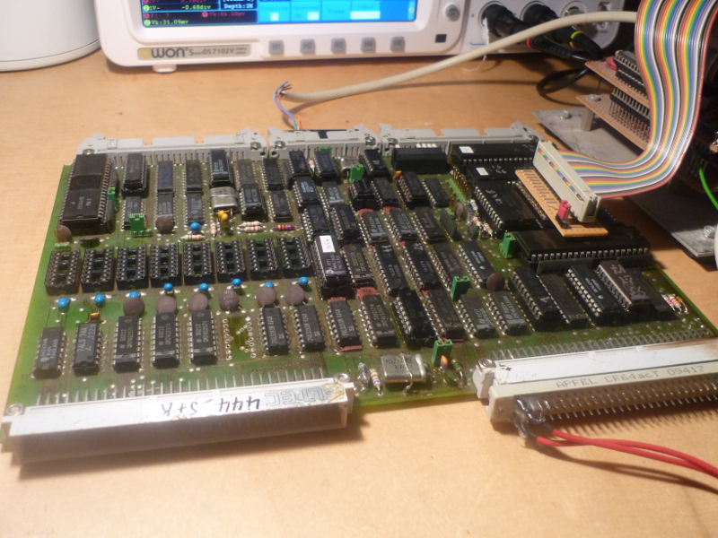
For my work on vintage electronics, I sometimes need a device programmer for (E)PROMs and PLDs my Labtool 48 cannot handle.
2708 EPROMs are one example, they need three supply voltages, 2532 EPROMs are another problem because of different pinouts between manufacturers and so on.

Therefore I bought a Data I/O 29B with an Unipak 2B adaptor some years ago on eBay – some more info and a photo here: http://en.wikipedia.org/wiki/Data_I/O)

The PC software for computer control mode was obviously not written with evolution in sense. I tried it on a Pentium III at 400MHz first, then on a Pentium MMX, but I got lots of transmission errors and timeouts although neither the COM ports of the PCs used nor the system 29B interface was bad.

Now I finally started the project to write a new, portable, GUI-based application to talk with the 29B.
The functions planned so far:

  • connect to programmer, request capabilities and report errors
  • select device from a list of supported devices, send family code to 29B and adjust memory buffer size
  • read from device to memory buffer and show checksums
  • write memory buffer to device
  • save memory buffer to disk
  • load file into memory buffer
  • verify device against memory buffer

Basic functions are already implemented, a 2708 is the only selectable device at the moment, which can be read and saved to disk. I use the default format MOS Hex (81) for data transfers from and to the 29B, which contains checksums for every record of 16 bytes which are compared with the actual data to make sure no transmission errors have occured. I have not yet checked what needs to be done to allow larger devices (>64k) to be handled with this format as it uses fixed 16 bit addresses, nor how 16 bit devices or even PLDs can be used.

The program is written in C++, using the Qt Creator as IDE and obviously Qt for GUI “artwork” and OS abstraction of serial and file I/O.
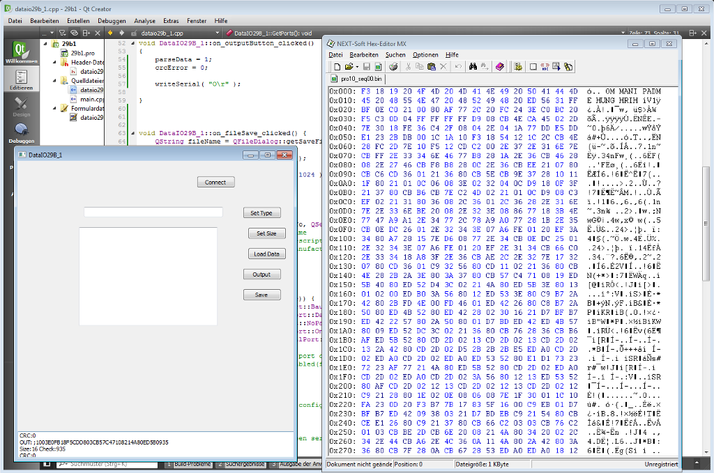
Here’s a very first impression, more to follow:


The hex editor on the right shows a file actually written with my program. The contents are from one of the Sequencer EPROMs of a SCI Prophet 10, by the way. Om mani padme hum!

Posted in R&D

The drawer – or what’s left

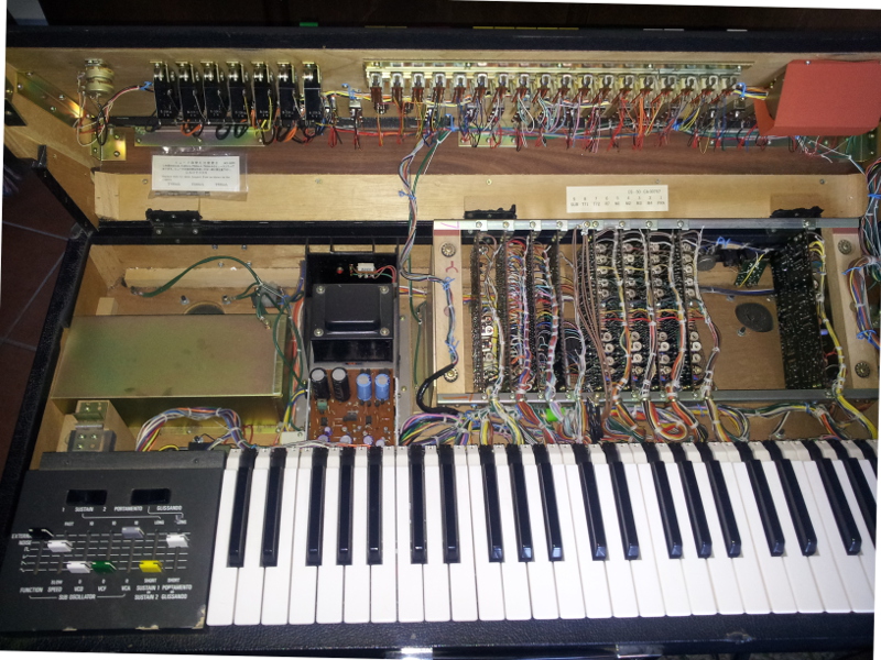
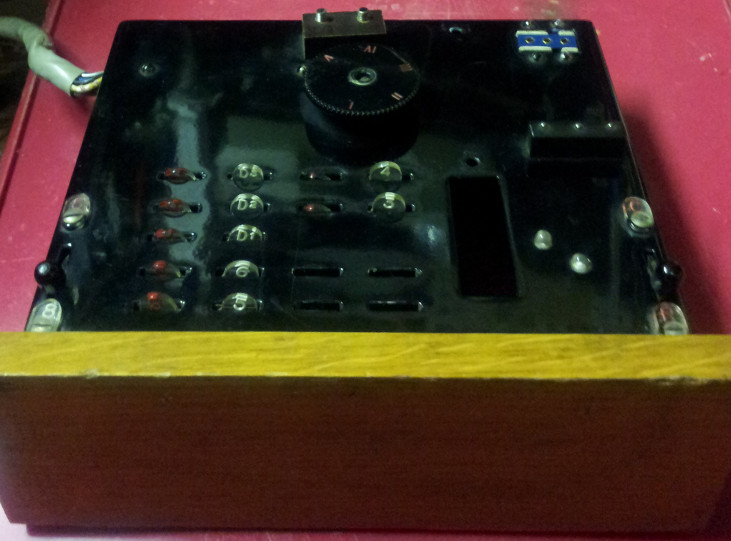
Here are some facts about the drawer – the control panel – of a Mk V Ondes Martenot.
Two swichtes (1, 2) are missing and the touche d’expression is absent as well. No fear, they are kept warm and cosy.
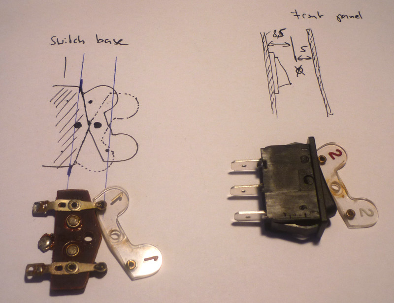
The switches are built from Pertinax (laminated paper) which has suffered over the decades, so that I will drop genuinity in favour of reliability and combine the old nice levers with 2013s switches.


The controls in detail, from right to left:

– switch C/R (rightmost) : selects between clavier (keyboard) and ruban (ribbon)
– three metal knobs : that’s for the circuit benders amongst the ondistes – here your finger becomes part of a series connection with a small capacitor,
directly influencing the oscillator.
– two transparent push buttons left from the C/R switch : transposes down by some amount (only in ribbon mode)
– the big rectangular hole normally hold the touche d’expession, the main volume control button of the Ondes
– switch 1 : adds a LC low pass into the D1 output (red – in, white – bypass)
– switches 2, 3 : some kind of tone control applied to the output amplifier (red – filter, white – off)
– switch 4 : determines the amount of 2&3 (red – full, white – attenuated)
– switch 5 : controls the gain of the pre-amplifier tube – probably into limitation, so a sine will become somewhat rectangular
– switch 6 : adds a filter to the metallic speaker (D2)
– switches D1, D2 & D3 : select the speaker(s) used. D1 is the main speaker, D2 the metallic (gong) speaker, and D3 the palme (with the strings)
– switch 8: adds a bridge rectifier into the signal for speaker D1, thereby doubling the frequency

The wheel numbered I..V : volume control for the main speaker (D1) – to adjust the balance between D1 and D2/D3

Polysix photocoupler myths

Many Polysix’ will be hit by a sudden photocoupler death somewhen.
There are many “facts” around on the internet describing how do determine whether it has failed and how to substitute the unavailable IC.

Fact 1: it is not true that you can check the photocoupler by measuring the voltage drop on the 4k7 resistor inseries with the LED or even the voltage drop across the LED.
LEDs do fail without exhibiting any dramatic change in electrical parameters. You will find LEDs which drop 1.6 volts @ 20 millamps and emitting no light!
(That – and some scientific applications – is why some applications still require incandescent lamps, and that’s why I’ve designed a controller for a 1960s filament winding machine in 2010!)

In this special case, the LDR saturated at 5.4 megohms with full LED current, so either the LED has become dark or the LDR insensitive.
The only way to check the photocoupler is to remove it from the circuit and measure the LDR resistance versus the LED current and compare it to a known working part (see diagram below)

Some background: the photcoupler is used in a feedback loop to stabilize the expo converter which makes up the V/Hz scale for the VCOs from the octave/V control voltage.
To use only one expo, Korg has used multiplexers to feed the 6 VCO CVs to the expo, followed by a calibration voltage and then the CV for standard pitch (only for the new production voice board).
The two latter outputs are routed to two independent controllers; the last one introduces an offset to the expo input to shift the standard pitch to its desired value, while the converted calibration voltage drives a current through the photocoupler’s LED, while its LDR is placed where you would normally expect the 3300ppm tempco resistor in similar circuits.

This leads to an eady way to check whether a tuning problem is related to the photocoupler circuit at all: measure the voltage on pin 7 of IC18. Within regulation it should be somewhat between -2 and -6 volts, -3 are more normal.
When the loop breaks open due to failure of the photocoupler or related parts, it will be stuck on the maximum negative output, something around -13 volts. There must always be a small current through the LED, otherwise the loop does not work and the TUNE HIGH preset has no effect!

Fact 2: the types VTL5C2 and VTL5C3 which are widely discussed as replacments are simply the wrong choice. In order to make the regulation work, the LDR resistance needs to be in the range of below one to a few kiloohms. The maximum LED current is limited by design to slightly over 2 mA. According to the datasheet, a VTL5C2 has 2 kiloohms at 2mA – regulation will never take place! Even if it seems to work, the controller will work close to the margin and operation cannot be guaranteed. Furthermore, resistance variation is quite large for those devices; the VTL5C2 I have tested had about 20kohms at 1mA.

The diagram below shows a known good original part (blue graph) and a VTL5C9 (yellow graph, values from the datasheet)
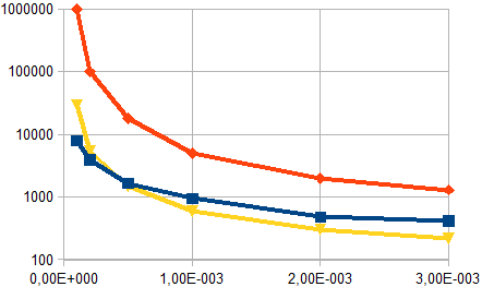
As you may have expected from my previous text, the red line represent the data sheet values for a VTL5C2.
While the VTL5C9 closely matches the original part in the most interesting region, the VTL5C2 resistance is way too high for any current.

What about RoHS…?

Photocouplers with LDRs are, as any LDRs which are commonly based on CdS (cadmium sulphide), forbidden for new products within the EU for some years now.
There is an exemption for the use in electronic music instruments, because there is no practical solution to control varying ac voltages better with LDRs.
(MOSFETs, for example, become highly nonlinear introducing distortion).

In this special case – a closed control loop and very small voltage variation across the device – a photo-mos device would probably be possible.

But it won’t be a solution for the control of audio signals in many applications. The EU has decided that science will have developed and indutry produces an alternative from december 31, 2013 on.
Science hasn’t, and industry doesn’t – except from Macron, who even try to force the EU to withdraw the exemption. Unfortunately, their devices are now way available at major european distributors by now…

Although it is always a good way to reduce hazardous substances, eurocracy has lost any sense of proportion for this topic. While power toys (sorry, I refuse to claim such crap tools) with short life spans flooding the market at low prices are allowed to contain batteries with large amounts of Cd, small photocouplers containg micrograms of Cd typically used in high-priced gear which will last for decades and serviced in case of a problem are to be banned.



Ready to fly!

After almost two years the SE1 mod is finished. Now intense testing can start.

Here’s a quick shot of the new inside. The aluminium back extension contains the six jack boards with all the audio signal amplifiers and CMOS switches. Those boards are connected to the analog PCB of the SE1X directly via shielded cables.
The control board for all the new circuitry resides on top of the SE1X digital and analog boards, shielded with a large copper-cladded FR4 sheet.


The new SE1X has 44 1/4″ jacks – somewhat more than the original two connectors. The meaning of the abbreviated information shown on the labels is explained on the very bottom of this page, so scroll down for a reference until I’ve finished the block diagram.

Cables!

Hopefully the last time I had to remove the back and all the modules for some minor fixes, the SE1X shows all its new wiring here.
The 4o wire ribbon cable has been tapped by the new controller board on top of the original boards. All switching signals and control voltages are handled here.
Shielded cable has been used to interface with the audio signals right on the analog board (which means removing some resistors and cutting some traces – ouch!)

All boards have been tested successfully now with this setup, two potentiometers turned out to be of wrong value for the possible parameter deviation and will be replaced soon.
Goooooooooooo!


But hey, what’s that?

(first of all, for the younger readers: this is a digital photo of an analogue scope screen, with a real cathode ray tube. Yes, I like those things when working with analog signals.)

The lower trace is the output of the RMOD gates (4070 CMOS device) with only VCO2 running, the upper is the triangle wave of VCO2 routed to the output.
First you might think this is a shot-through of the VCA controlling the RMOD amount to the master mix – nope, it is not.
It’s the hard switching of the 4070 causing a spike on the +10 volts rail, making its way into the analogue circuitry.

I’ll have to think about that later.

Lexicon PCM42

What we’ve got here is a Lexicon PCM42 delay unit which some techs have already been working on.
While the inital problem was some kind of distortion, the delay path was pretty messed up when it came to me. Well below the yellow LED of the input level indicator was lit the input signal to the A/D converter was heavily clipped.

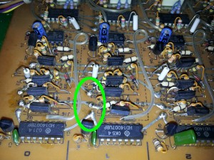
It became clear very soon that the unit uses some kind of compression/expansion technique to virtually increase the A/D and D/A resolution, similiar to A-law or µ-law used in telephony as well as by other music applications realized by simple non-linear amplifiers built around a RCA CA3039 diode array. Some measurements made sure that those diodes were actually not where they’re supposed to be. I did not care whether a defective (how should that be – the array is connected via rather high resistors to the circuit preventing excessive current flow) or fake CA3039 was causing this but ground the thing open:

What we see here is obviously not a fake, but a very dead CA3039. One single diode junction has survived, and judging from the vaporized bond wires, the current must have been rather high – much higher the circuit ever allows.

On further examination I found serveral component leads being clipped and soldered back together, maybe to measure those parts out of circuit.  Some copper tracks have unfortunately been damaged too.

A rather important 2.55kOhms resistor has not been reconstructed so I decided to restore the unit before doing the actual trouble shooting. After the resistors, capacitors, two diodes, the CA3039 and a LF356 that has previously been identified to be defective had been replaced.

A first test probably showed the initial problem with the PCM: the delayed output was clipping on one half wave at any input level.
Some signal tracing revealed that very first op amp followng the Am6012 DAC in the reconstruction (read: D/A) path showed a 0.6 volts DC offset on the output, way too much to be compensated by the offset trimpot.
Now there were not many parts left to be checked: the Am6012 DAC chip, the output resistors and the op amp itself. The latter one was easily ruled out by swapping, and as I did not have a AM6012 handy, I checked the resistors. Et voila: each of the two DAC outputs is pulled to an internal +10V reference by two paralleled 10k resistors, being part of a 8x10k DIP array. While 7 of the resistors were well within tolerance, one measured this:

This is more than enough for the measured offset voltage. After replacing the resistor pack by 8 precision resistors the delayed output was clean, symmetrical and free from clipping.
Once again cleaning up after some other’s repair attempts was much more costly than the repair itself. But the most important thing is that a great piece of studio equipment is alive again!

Ready again…

Recently I checked the mod boards in the SE1X to find out that there still was some level mismatching. The intended 0.775 volts RMS on any stage output and external input were not yet achived.
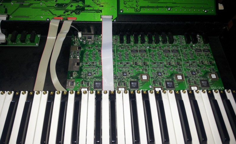
So I removed the boards and did some additional modifications. Here’s a photo of the updated boards. No, these are not the boards for 6 SE1X’s but the complete mod for one single unit!
And it’s not even the full mod, the controller board shown above as well as some meters of additonal wiring belong to the upgrade too.

During re-assembly I will check the levels starting at the VCA back to the VCOs and have the last missing parts installed, once the required values have been determined. Stay tuned!

Stacking it up

As circuit design is finished and most PCBs are populated now, it’s time for assembly.
First of all the controller boards need a place:

Here you can see the Controller Board on top of the original SE1X CPU and analog boards.
An additional copper-cladded PCB should prevent digital noise from the new microcontroller to disturb the analog board, although the small ATmega @1MHz with no fast clocked outputs would not make much EMC trouble either. The Controller Board gets its +/-15 volts supply directly from the PSU, all other voltages (+/-12, +/-7, +5) are generated on board.

The board lying on the table is one of three VCO jack boards. The functions of its 8 jacks is alrady outlined in the previous post.

I thikn it’s time to wire & fire things up…

The MIDI jacks from the SE1 CPU board have been removed and extended by shielded cable to allow the DIN jacks to be fitted in the new rear panel, same will apply to the IEC power connector.
Yes, it’s supplied from an isolation transformer, and yes, the open frame PSU is a nasty little devil and will be replaced by something more safe and silent.

The VCO1 Jack Board is now connected to the Controller Board by several (yellow) cables, carrying control voltages of different kind. The two shielded cables are hooked up to the analog board – one in between the VCO output and VCO Amount VCA input, the other one delivers the triangle output to the sine converter on the Jack Board. The sine wave is mixed to the VCO output under control of the Controller Board, eventually overriding the command from the SE1 CPU.

On the photo above I was adjusting the Middlebrook & Richer triangle to sine converter that any of the 3 VCO Jack Boards features to allow all three VCOs producing sine waves. I was quite surprised that I got the 2nd harmonic down to -50dB and the 3rd to -40dB, measured at 440Hz. Overall THD will be in the 1.5% range, maybe even better when final adjustment are made.


Synclavier Sample-to-Memory – getting serious…

The NED Synclavier is an awful combination – complex circuitry built up of hundreds of (mostly TTL) ICs and no documentation in the wild.

So there’s no way around getting intimate with circuitry to understand how things work to make my latest project possible. First of all I needed an idea how everything is timed – a most important point in a serially operating system. Similar to the Able processor itself, the Sample-to-Memory unit makes use of an unidirectional 16 bit parallel bus on which control information, memory addresses and finally data are sequentially transfered.

All information propagate through the daisy-chained modules PSF, PSADC, PS(B)MC, DDDAC and then back to PSF, while the four timing signals into which all communication is framed traverse the chain in the opposite direction. To learn how this actually works, I’ve hooked up a minimal memory chain setup consisting of only the PSF and a PSMC. As the PSF gets the actual timing from the PSSRGA, the latter board is also installed in the poly bin:

The analyzer probes bring some color into the bin.

It was a quite succesful session so far, the bus timing is no secret to me anymore.

Stay tuned for the next steps on a long way…