KORG PS3x00 Series MIDI Interface

Here I want to introduce my approach to MIDIfication of the KORG PS3x00 series. It is not really different from previous solutions, but for me it has the advantage of being available when I need one.

The features:
– MIDI In only
– drives the 49 key contacts with the full voltage swing
– allows for program change in the PS3200 synthesizer
– has 8 1/4″ outputs, routed to an external breakout box featuring also the MIDI connector and a “learn” button to set parameters
– 6 of the analog outputs can be unipolar (0..+5V) or bipolar (-5..+5V) or a simple 0/+5V switching function and assigned to any MIDI CC
– 1 output is mapped to pitch bend with 14 bits of resolution
– 1 output is mapped to modulation

Here are some impressions of the prototype

PPG Multicontrol Keyboard (323)

Featured

The PPG digital keyboards were a completely new approach in controlling analog modular synthesizers. While most other manufacturers(*) used resistor strings, sample&hold circuits and eventually means of analog computation to achieve polyphony, Wolfgang Palm of PPG went the digital way. This allows for completely new voice assignment schemes and complete pitch stability after a key is released.

The references I found vary a bit in functionality. A Duophonic Keyboard 322 I found on the web for example has one switch setting for monophony, duophony, split mode and a button-activated memory mode, which is also described in the “INFO MAPPE SYNTHESIZER MODUL SYSTEM 300er SERIE” from December 1976. Also in this publication there’s a photo of a multicontrol keyboard similar to the one described in this post.

It came to me in parts, with lots of the internal wiring cut and rewired for some unknown purpose. The goal is to restore full original function, while adding the previously removed internal power supply, and to reverse engineer all of its circuitry to create some documentation also for its usage from this.

(*) Oberheim used a digitally scanned keyboard around the same time in the FVS, but there are probably not many more examples.

Before I start over with individual posts showing the functional units of the keyboard, here is a first impression of how it came to me and how important a careful disassembly, documentation and restoration will be.

Keyboard electronics

The keyboard is based on a rather typical J-wire style keyboard. 49 J-wires are sequentially pulled to ground by means of a counter/decoder circuit on the keyboard assembly itself. This is synchronized by several signal lines with the keyboard assigner circuit on one PCB below the left hand control panel.

Circuit description

For all circuit descriptions I will use my redrawn schematics attached to the post. The part designators are randomly chosen as none of the original PCBs has component designators of any kind.

The whole scanning of the keyboard including the storing and assigning of key data is clocked by a 555 timer IC running at 14.6kHz with an almost symmetric output. This clock is fed to the assigner circuit by the grey wire connected to pin 6 of the multi-pin connector. Simultaneously it clocks a cascade of two SN7493 4-bit counters.
They are arranged that 6 outputs define 64 time slots of 68.5µs, so a whole scan cycle takes 4.4ms. The lower three bit are connected to the ABC inputs of 7 SN7445 BCD decoders, while the upper three drive another SN7445 which in turn enables one out of the 7 other 7445. As the Q0 output of the latter 7445 is unused, the actual keys are mapped to the time slots 8 to 56.
The last decoder output, which goes low in the 63rd time slot and is used for synchronization purposes via the blue wire on pin 9 of the connector. Additional timing information is derived from the 6th bit of the counters (U3 pin 8) which, via the white wire on pin 1, indicates whether the lower (key 1-24) or higher (key 25-49) half of the keyboard is currently scanned. This is obviously necessary to allow for split assignment.
U3 pin 11, the 7th bit which is not used for the keyboard itself, is also sent via pin 2, brown wire, to the assigner circuit. This plays an important role in the control circuit for the key memories as the actual key data is only interpreted in every other scan cycle, so the real scan time becomes 8.8ms rather than the previously mentioned 4.4ms. The pink wire on pin 7 carries the actual key data, it becomes low for every timeslot in which the associated key is pressed.

Schematic of the keyboard circuit

Key assigner

The key assigner allows to generate two independent control voltages and gate signals from the time multiplexed data from the keyboard circuit. Each output can be selected between two monophonic, two duophonic and two key-split modes with a fixed split point between key 24 and 25 (see above).

To achieve this, the pulse train from the keyboard is stored in two 64 bit serial shift registers (Texas Instruments TMS3417). Those are controlled using the synchronization signals from the keyboard circuit, the mode switches on the front panel and a circuit defining whether the real time keyboard data or the recirculated output is fed into the registers.
The shit register output, together with additional control signals, are fed to a second PCB which converts the pulses (not parallel digital data!) to the precise control voltages.

A detailed circuit description follows.

OB-Xa auto tune demystified

Recently a half repaired OB-Xa hit the workshop. The main trouble was complete failure to auto tune. After fixing some obvious faults (damaged vias, poor quality trimpots) the auto tune issue remained. Although the serial number indicated “old” auto-tune the program LED advanced during auto tune, so the firmware has been upgraded to a revision C already.

Until now I have always ignored that the service manual does say that the Revision C software has a new auto-tune circuit – so I had to learn it the hard way. I measured the gate time of the period meter circuit (which is around 3.82ms for a well tuned VCO, 4 periodes of a high C at 1046,5Hz), measured the clock frequency which is half the crystal clock or 2.4576 MHz. This gives a period count of around 9400.

Now I disassembled the firmware and saw that the target count is not in the 9400 range, but twice of that – 18,788 ! I verified my assumptions by feeding a 523Hz clock from a DDS generator which instantly let auto-tune pass.

During this, I also used the great “XACA2” patch EPROM from Ricard Wanderlöf (read here http://butoba.net/homepage/synthhacks.html). We had an email chat for some days trying to evaluate what is happening and came to the conclusion that all out assumptions must be right and that there must be a hardware change as well.

But first my comparison between the XAAD firmware (the last of Revision A) and the XACA disassembly:

While the Revision C compares the period count with 18,788, the old revisions indeed had a target value half as high!

So the only solution to this can be that the period meter is clocked from the full crystal frequency of 4.9152 MHz for Revision C and higher. Half an hour(!) I made this conclusion I found the ECO #119 which explained how to change the upper board for use with the Revision C firmware.

Some times we learn it the hard way. Lots of techs I asked during the process weren’t aware of the hardware modification – or just forgot about it, 40 years later…

Interesting enough: the original schematics of the later mainboard type for the Revision F and G firmware still show the period meter clocked by 2.4576MHz, while the target value in the firmware remains at 18,788. So this must be an error in the diagram, probably not the only one.

Here’s the ECO #119:

ProPSU – a PSU Upgrade for the Prophet 5

The SCI Prohet 5 Synthesizer has thermal issues in the power supply. SCI’s attempt to make do with a single CT secondary winding results in a voltage of up to 25VDC before the 7805 series regulator. The lack of a decent heatsink makes this even worse. Several techs have been rebuilding the stock PSU with either an additional tranformer or by replacing the transformer with a new one with an additional winding, supplying around 9 volts to an additional rectifier.

This modification also requires some work on the reset circuitry, otherwise the RAM contents might be damaged on shutdown. Other typical work covers replacing the thermal interface material, the big filter capacitors and the tantalum capacitors on the PSU board.

I decided to somewhat standardize the PSU maintenance of Prophet 5’s by designing a drop-in replacement PSU board I called the ProPSU. In order not have to temper with the name plate I made a aluminium heat spreader that is tightened to the back (use of some thermal compound is highly advised!) by re-using three of the original screws. The ProPSU board itself will be, after the cable harness is soldered to the ProPSU, bolted to the readily attached heat spreader by means of 3 or 5 M3x16 machine screws.

The ProPSU can be used for both Rev.2 and Rev.3 Prophet 5’s, with either the +12/-5 volts rails for the 2708 EPROMs provided or missing. Both 15V supplies can be adjusted by means of multi-turn presets. An on-board reset circuit switches the “+20V” rail to the mainboard’s reset generator, simulating a quickly discharging filter cap when the +5V supply drops below 4.75 volts. On turn on, the delay of the reset circuit ensures that all voltages are stable.

propsu_top

Ready to use ProPSU for late Rev.3 or modified Prophet 5 (new EPROMs, no +12/-5V required)

propsu_mount

Mounting detail: the heat spreader bar is attached to the bolts of the old PSU’s regulators, after that the ProPSU
PCB is mounted to the heat spreader (isolation washers not shown here)

APR Odyssey: CV/Gate for the White Face

Several approaches of adding CV/Gate to the Mk I Odyssey consist of not more than 3 or 4 1/8″ jacks with switch contact that interrupt and hook into the internal CV, gate and trigger lines. While the CV uses standard 1V/octave, the gate and trigger signals require a rather high amplitude of about 10 volts, with the additional impact that the gate level has a direct influence of the achievable output level of the AR envelope. Furthermore, both gate and trigger signals are needed for most modifications.

By adding a simple transistor circuit that resembles the levels generated by the Odyssey’s A board this ARP now works perfectly even with 5V gate and trigger levels and does not require the separate trigger signal anymore, although the trigger input jack is still provided for special purposes.

Odyssey Gate CV

The prototype for the improved CV / Gate modification in action


PPG 390 Drum Unit

One of the most rare PPG units found its way to my workshop recently: the 390 Drum Unit.
PPG 390 Drum Unit

Basically, this is a very rudimentary 8 bit sample player. It features 8 drum sounds in EPROMs on 4 voice cards. Two clock sources drive the address counters on the boards, which means that Sample Freq 1 defines the sampling rate of the odd channels, while Sample Freq 2 is in duty for the even numbered instruments.
[Block diagram to follow…]

Upon arrival one card was missing, instead I found a non working wire-wrapped vero board with a prototype for a single 4kByte instrument in two 2716s, and two 2732 EPROMs with instruments samples that won’t fit anywhere. I designed a PCB to replace the missing voice card, providing sockets for 2764 EPROMs so experimenting with other samples woule be easier as they can be programmes with cheap USB programmers.

PPG 390 Voice Card

Once completed the design I realized that I cloned the original cards so perfectly that I still don’t have a use for the 2732s – but my layout provides an easy solution, with two piggy-packed 4040 counters and some wires I modified my new voice card to work with the Noise and Hi-Hat EPROMs. Some more wires would allow to experiment with 2764 or even bigger EPROMs.

The clock frequencies are in the range of 13 to 30kHz, so the sound duration is between 70 and 160ms for the originally used 2716 EPROMs and 140 to 320ms for the 2732 sounds and would scale accordingly when using a larger EPROM.

PPG 390 Overview

Apart from this addition, the cards got guides (the blue things) to protect the connectors, new capacitors, additional capacitors in the output lines (originally it had a 3V DC offset), a new transformer, IEC mains jack, a mains fuse and a mains wiring according to current standards.

It is probably not an impressive drum unit sound-wise, but an interesting collectors item and I somewhat like the shaker … 😉

Posted in PPG

Advancing the Synthex

Four years ago I wrote “except the LFO section, because it’s strictly analogue”, but this did not really let me rest. So I started designing a new LFO board with some special features that can be controlled by the new processor board that is currently in development.

While the processor board design is near completion, a first prototype of the Advanced LFO has just entered the programming phase. Here’s a peek for those who are following the project for some time now. It’s alive!

Advanced LFO Board

PPG 1020: Digital keyboard?

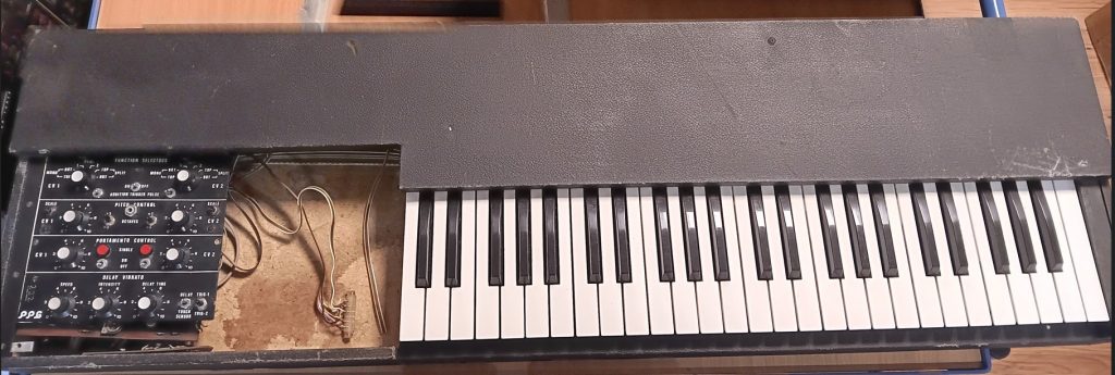
The PPG 1020 is known as the stable successor of the 1002 synthesizer. This was achieved by use of a special oscillator architecture that combines digital octave division and a closed-loop approach including a VCO. The VCO covers the whole range(4 keyboard octaves + approx one more for the “digital modulation” feature), but being within a closed loop, it is stabilized to some degree. The details will be topic of a later blog post. For now we only need to know that we need a digital word that determines the octave and a control voltage to drive the VCO to one out of 12 semitones.

Even without the use of a processor (the 1020 does not have a computer of any kind) it would be straight forward: scan the 49 keys, somehow divide the number of the pressed key modulo 12, the result will be the (already digital) octave number, the remainder drives a DAC to generate the CV.

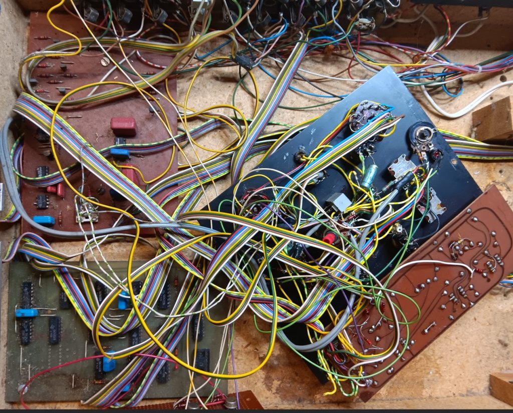
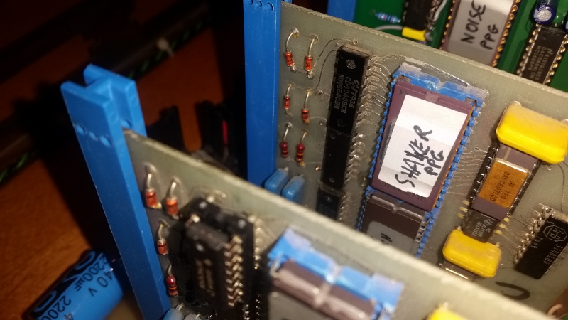
This “somehow” was actually done by using synchronously counting registers – a chain of 2 binary counters, one turning over at 12, the other incrementing whenever the first one turns over, and a chain of shift registers scanning the keys. The first “high” (pressed key) in the serial pulse train from the shift registers will latch the counter outputs in the next cycle, so we have a low-note priority here.

The counters mentioned above drive the octave control word and a digital-to-analog converter built from two 4051 multiplexers and a chain of accordingly weighted resistors. The reference voltage to that chain is generated on the main board and derived from the setting of the tune knob and the pitch bend slider.

For modulation purposes, an offset is digitally imposed. Since the modulation source from the main board is an analog control voltage, analog-to-digital conversion is necessary. A discrete A/D converter was built from a constant current source generating a linear voltage ramp on a capacitor. This slope is than compared with the modulation voltage in order to reset the above mentioned counters, thereby shifting the generated octave control word and the control voltage. With this approach it is possible to modulate the pitch across an octave border, whereas the analog part of the oscillator control would be limited to variation within an octave.

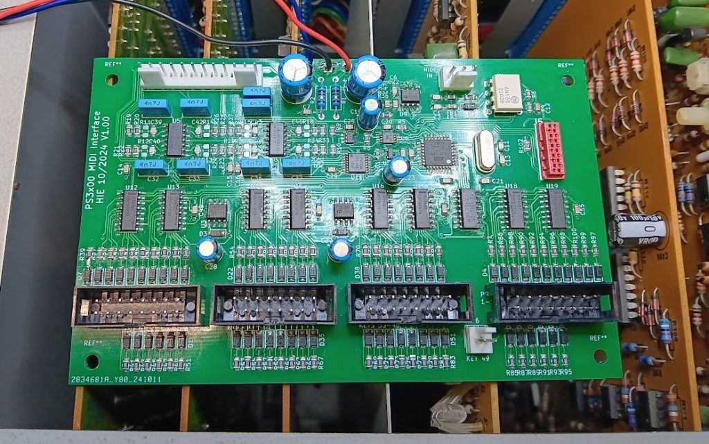
The comparator in this A/D converter is built from discrete transistors, yet integrated into a CA3086. The same circuit, but under processor control, can be found on the analog panel board (ANIN) of the Wave Computer 360!

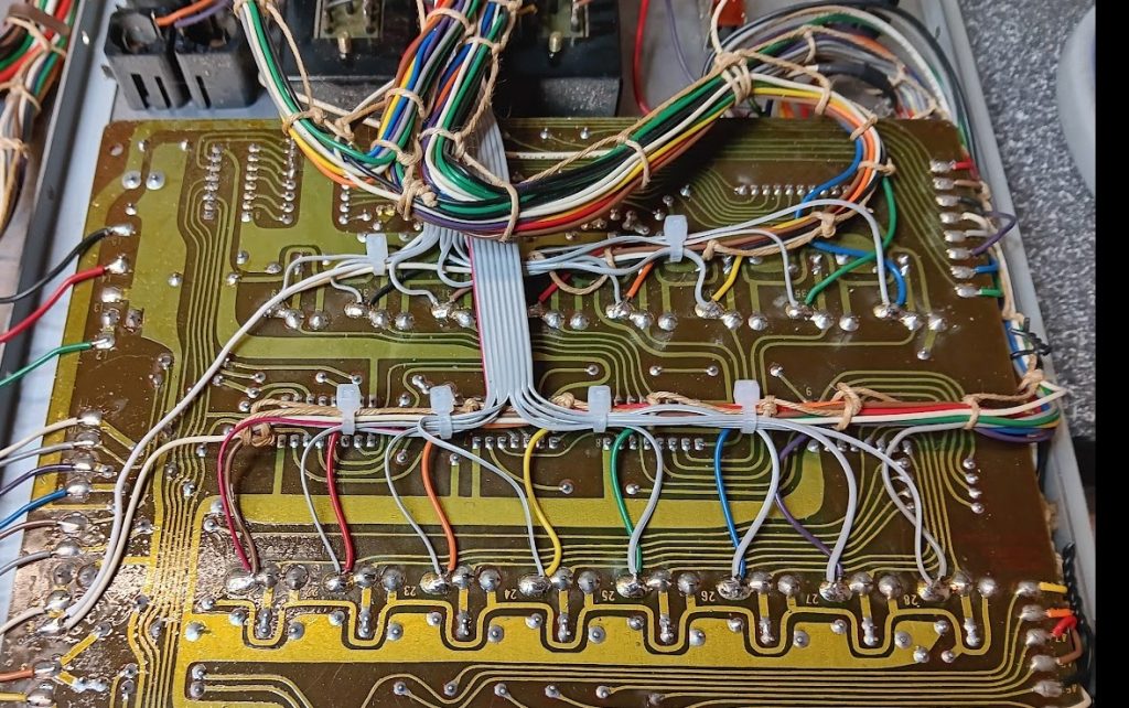
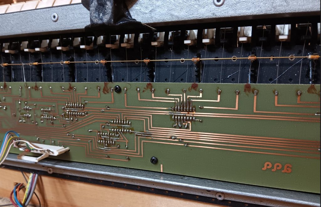
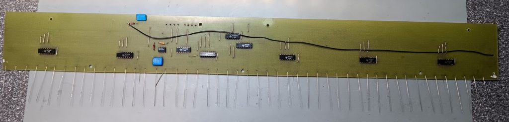
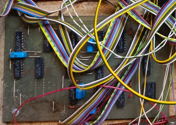
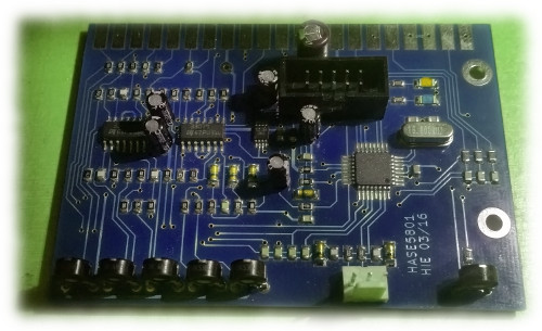
Here’s the component side of the keyboard PCB:
PPG 1020 keyboard PCB components side

While the copper areas in the right top and middle right are of no electrical use, the long copper stripe on the lower edge is actively driven by a delayed clock signal. One might wonder what the reason for this could be – a view on the solder side and some circuit analysis reveals the secret:
PPG 1020 keyboard PCB solder side

Every key has a 2x1cm big copper area connected to the J-wire on the opposite side. Electrically, each key is capacitively coupled to a delayed clock signal – a signal that is logical “0” whenever the shift registers sample the key lines. This loose coupling is easily overriden by a J-wire touching the bus bar, which is connected to the positive supply voltage by a resistor of just 1k.

The last question about this is: was this only done to eliminate the need for 49 pull down resistors (the shift registers are CMOS devices and would not work properly with open inputs), or were other aspects like debouncing in mind?

A 3.3meg resistor added between one key line and ground suggests that the capacitive pull-down idea did not work 100%.