PPG Multicontrol Keyboard (323)

Featured

The PPG digital keyboards were a completely new approach in controlling analog modular synthesizers. While most other manufacturers(*) used resistor strings, sample&hold circuits and eventually means of analog computation to achieve polyphony, Wolfgang Palm of PPG went the digital way. This allows for completely new voice assignment schemes and complete pitch stability after a key is released.

The references I found vary a bit in functionality. A Duophonic Keyboard 322 I found on the web for example has one switch setting for monophony, duophony, split mode and a button-activated memory mode, which is also described in the “INFO MAPPE SYNTHESIZER MODUL SYSTEM 300er SERIE” from December 1976. Also in this publication there’s a photo of a multicontrol keyboard similar to the one described in this post.

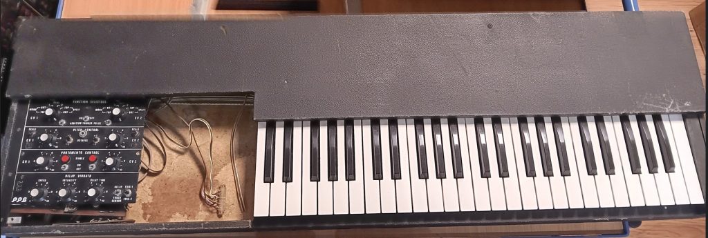
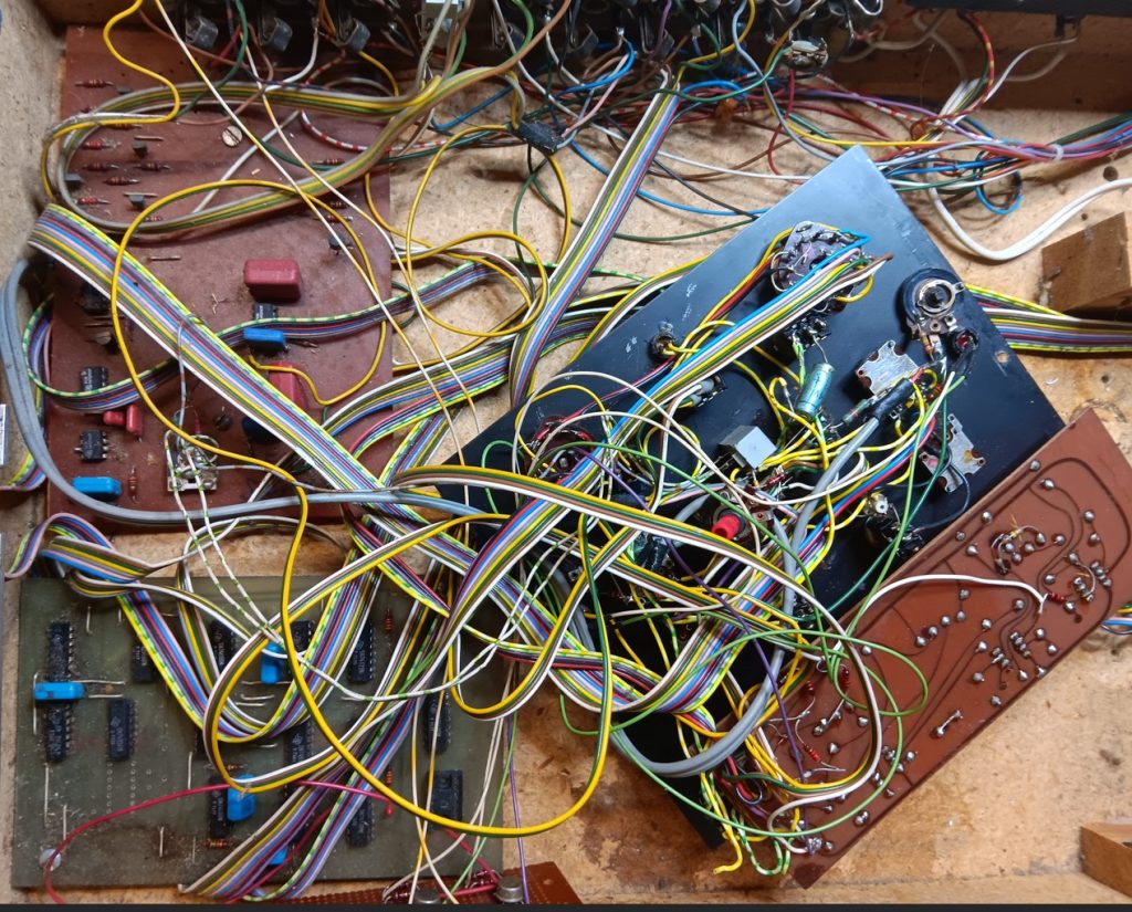
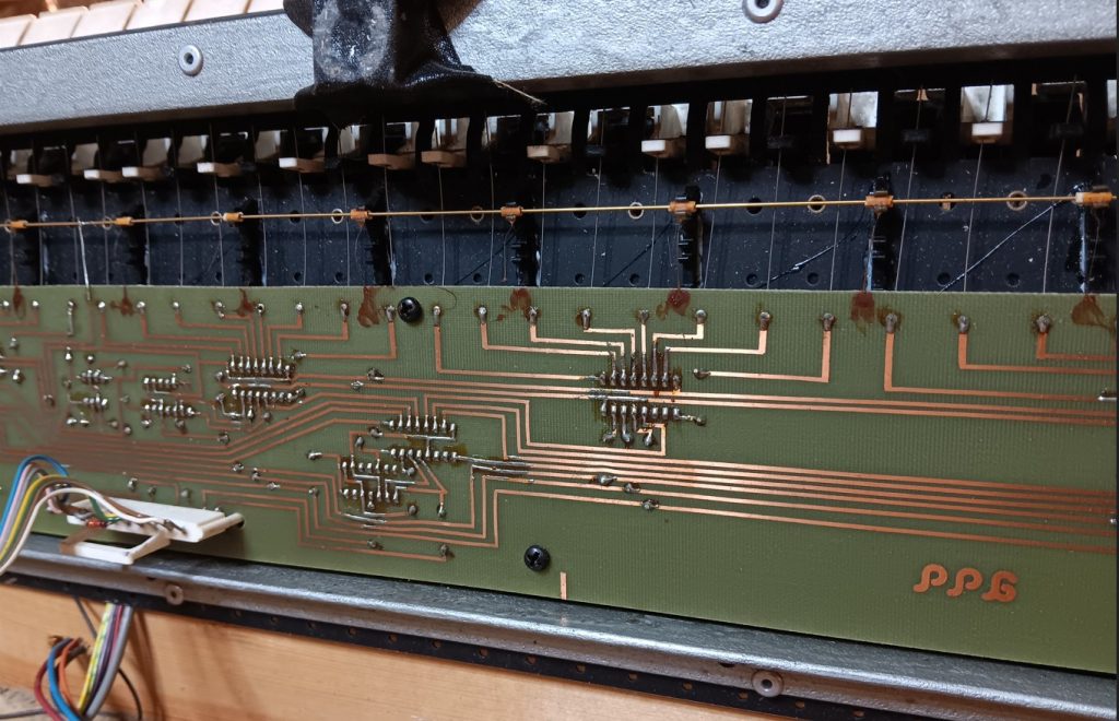
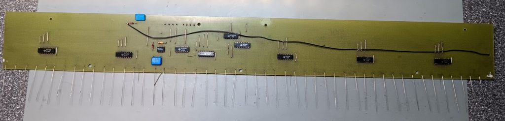
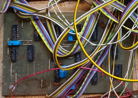
It came to me in parts, with lots of the internal wiring cut and rewired for some unknown purpose. The goal is to restore full original function, while adding the previously removed internal power supply, and to reverse engineer all of its circuitry to create some documentation also for its usage from this.

(*) Oberheim used a digitally scanned keyboard around the same time in the FVS, but there are probably not many more examples.

Before I start over with individual posts showing the functional units of the keyboard, here is a first impression of how it came to me and how important a careful disassembly, documentation and restoration will be.

Keyboard electronics

The keyboard is based on a rather typical J-wire style keyboard. 49 J-wires are sequentially pulled to ground by means of a counter/decoder circuit on the keyboard assembly itself. This is synchronized by several signal lines with the keyboard assigner circuit on one PCB below the left hand control panel.

Circuit description

For all circuit descriptions I will use my redrawn schematics attached to the post. The part designators are randomly chosen as none of the original PCBs has component designators of any kind.

The whole scanning of the keyboard including the storing and assigning of key data is clocked by a 555 timer IC running at 14.6kHz with an almost symmetric output. This clock is fed to the assigner circuit by the grey wire connected to pin 6 of the multi-pin connector. Simultaneously it clocks a cascade of two SN7493 4-bit counters.
They are arranged that 6 outputs define 64 time slots of 68.5µs, so a whole scan cycle takes 4.4ms. The lower three bit are connected to the ABC inputs of 7 SN7445 BCD decoders, while the upper three drive another SN7445 which in turn enables one out of the 7 other 7445. As the Q0 output of the latter 7445 is unused, the actual keys are mapped to the time slots 8 to 56.
The last decoder output, which goes low in the 63rd time slot and is used for synchronization purposes via the blue wire on pin 9 of the connector. Additional timing information is derived from the 6th bit of the counters (U3 pin 8) which, via the white wire on pin 1, indicates whether the lower (key 1-24) or higher (key 25-49) half of the keyboard is currently scanned. This is obviously necessary to allow for split assignment.
U3 pin 11, the 7th bit which is not used for the keyboard itself, is also sent via pin 2, brown wire, to the assigner circuit. This plays an important role in the control circuit for the key memories as the actual key data is only interpreted in every other scan cycle, so the real scan time becomes 8.8ms rather than the previously mentioned 4.4ms. The pink wire on pin 7 carries the actual key data, it becomes low for every timeslot in which the associated key is pressed.

Schematic of the keyboard circuit

Key assigner

The key assigner allows to generate two independent control voltages and gate signals from the time multiplexed data from the keyboard circuit. Each output can be selected between two monophonic, two duophonic and two key-split modes with a fixed split point between key 24 and 25 (see above).

To achieve this, the pulse train from the keyboard is stored in two 64 bit serial shift registers (Texas Instruments TMS3417). Those are controlled using the synchronization signals from the keyboard circuit, the mode switches on the front panel and a circuit defining whether the real time keyboard data or the recirculated output is fed into the registers.
The shit register output, together with additional control signals, are fed to a second PCB which converts the pulses (not parallel digital data!) to the precise control voltages.

A detailed circuit description follows.