Solina String Ensemble

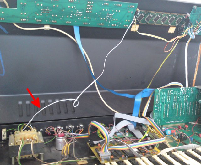
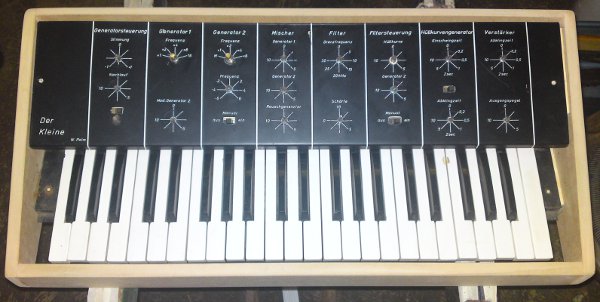
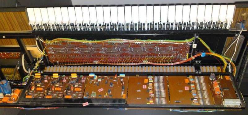
These days a Mk.I String Ensemble made its way on my table.
While working perfectly without the ensemble effect, it showed some heavy noise and reduced volume in ensemble mode.

The noise turned out to be a defective TCA350Y BBD chip. While I’m waiting for the replacment part, I checked the other two delay circuits and found one showing no output at all. Fortunately only a transistor in the astable circuit driving the BBD’s clock inputs was intermittent, so all transistors of this type will now be replaced to prevent further trouble.

There were several types of this instruments available under different manufacturer labels – Solina, ARP and Eminent. The earlier models used TCA350Y BBDs while the latest had TDA1022s.

Consumer Information

(for the case your String Ensemble is missing one or more certain notes…)

At least three different top octave synthesizer chips (TOS) were used: M087, SAA1030 and TMS3616. All of those could be replaced by my universal replacement module RPLTOS or RPLTOS+.

Read more about this little board here http://huebnerie.de/index.php?article_id=14 (in German language)

Wave 2 DRS Adapter

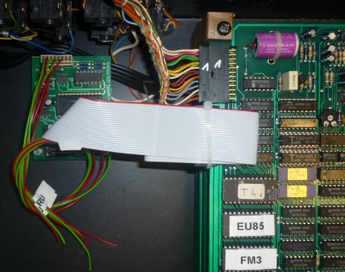
The PPG WAVE2 DRS ADAPTER – demasked

First a short summary of the jacks and switches:
On the left we have 6 phone jacks labelled A to F, one named START/STOP
and a 5pin DIN connector for TAPE SYNC.

Three switches allow to enable a click sound (there’s a small speaker in the DRS box), one to choose between internal or external clock and another to select whether the clock outputs shall be 3 or 4 times the internal timebase.

The phone jacks on the bottom invite the user to feed either a contact-closure or positive voltage trigger signal, the third one labelled INPUT needs to be connected to  the trigger in jack on the Wave 2 – there’s no trigger input pin on the 14pin Amphenol connector, only an output!

Before I start with the description of the 5 right side jacks named CL.1 to CL.5 I’d like to tell all those people who can’t wait to hook this adapter to their Wave 2’s not to have too great expectations, or probably learn some 6809 assembly language.

No, let me start with the bad news instead of the clock outputs. The inputs A-F on the left are not connected within the box. The resistor pack which would close the circuit between the jacks and some port pins of the Wave 2’s VIA chip (which are, for those who really want to hack the firmware, the pins PA4..7 and PB0..1) is not fitted and has never been there.

Furthermore, no known firmware for the Wave 2 – and we know three different versions at the time of writing – has a single line of code that communicates with those port pins in any way.

Now let’s have a look at the circuitry that actually could work.
For understanding it is helpful to know that the Wave 2 has a programmable triple timer chip, a Motorola 6840. Timer #3 generates a clock signal that is normally fed to the clock input of Timer #1 through a 10k resistor. This allows to either tap the internal clock, or to override Timer #3’s output to force an external clock to become the clock source of Timer #1 and thereby control the clock for sequencer, arpeggiator and maybe other functions.

This mixed output/input is connected to the DRS box and directly available on the record out pins of the 5pin DIN jack for tape recorder connection. This allows to record the internal clock to a tape or cassette. In addition the clock signal is routed to two frequency dividers: one, dividing by 8, is selected by the clock switch in the x4 position. By using some advanced mathematics, I was able to calculate that the clock signal generated by Timer #3 is 32 times of … something.
For the x3 position of this switch, Wolfgang and his guys made quite some effort so the x3 clock scaling must have been very important. The clock signal is divided by a binary counter that resets itself when reaching a value of 11, but this would be a little bit too slow to reach 3 times the base clock (32/11 is less than 3, q.e.d.), so the counter is additionally reset whenever the counter of the by-8-divider reaches a value of 32. This way a mean frequency of 3 times something with some jitter is achieved.

Whatever the x3/x4 switch selects is buffered and shows up on the jack CL.1 at 5Vpp. CL.2 to CL.5 carry the clock from CL.1 consecutively divided by 2, 4, 8 and 16. That’s all. It’s up to your imagination what you could do with 3 or 4 times the internal sequencer clock. The CL.4 signal, namely 1/2 or 3/8 of the sequencer clock, makes the speaker click unless told not to do so by the CLICK switch.

If you have recorded some signal to a cassette, you would be able to send it back as the sequencer clock through the DRS box.
The playback pins of the DIN jack are followed by a detector (as simple as a CMOS Schmitt trigger) and a buffer which overrides the clock input of Timer #1 when the switch is set to EXTERNAL.

Finally there’s a START/STOP jack. It’ driven by an inverted version of the CA2 pin of the Wave 2’s VIA chip. When the sequencer is stopped, this pin goes high, disabling all the internal circuity of the DRS box – the counters of the frequency dividers are kept in reset state, and all outputs are forced low, including the tape recording output and the clock jacks.  The START/STOP output is low in this state. It goes high when CA2 becomes low, which is whenever the sequencer is started.

For those who still want to know everything about this little box, here’s the mapping between VIA pins and jacks:

A -> PB0
B -> PB4
C -> PA7
D -> PA4
E -> PA5
F -> PA6

Creamware A16 DC modification

Honestly – serious production with Midi-to-CV to control analog synthesizers seems to be impossible. 7 bits translates to quite large steps in the control voltage. But how about using an studio grade 18 bit A/D – D/A box driven via ADAT?
If a Creamware A16 comes into your mind, you’d better think twice about it. There are some reasons converters like this are hard to modify for precise DC:

  • First of all, the inputs are capacitively coupled. But of course it can’t be as easy as just bypassing the caps…
  • Both the ADCs (Philips SAA7367) and the DACs (Philips TDA1305) use single +5V supply. This implies that the analog signals need to be centered around an internally generated reference voltage
  • The reference voltages are not quite precise. Although their long-time stability is very good, the initial accuracy is 5% or worse. Therefore also the signal range varies from chip to chip.
  • The ADCs have an integrated high pass filter to remove DC offsets, but fortunately it can be easily disabled by lifting up one pin and strap it to ground

The engineers saved some parts by not subtracting the DAC refence voltage from the outputs, but lifted the ground potential of all 32 jacks by the reference of the first DAC (channels 1 & 2). For this purpose, a high power voltage follower with massive decoupling on the output was designed. As the reference voltages differ from DAC to DAC, this approach would not work for DC, so I removed the circuitry and connected the jack ground to circuit ground.

When I was working on the PSU – a quite strange design by the way – I modified two regulators to supply +/-7.5 volts to the op amps because in the original design the op amp supplies were a) somewhat too low and b) shifted by the same amount the jack grounds are lifted beyond ground.

A last modification to the PSU applies to precision and stability: the analog supply which influences the reference voltages was derived from a LM317’s output by means of a voltage divider and a power voltage follower – including thermal drift. To improve the absolute precision of the converters, I replaced the resistive voltage divider with a TL431 shunt regulator.

But things became even worse…

While doing some measuring with the ADAT in and out jacks connected I found that the outputs are inverted with respect to the input voltage. With an ADAT box and appropriate software I was able to determine that the inversion takes place between ADAT-In and the analog output of the DACs, so another inversion in necessary here, including subtraction of the reference voltage.

This was accomplished by inverting the reference output of each DAC chip (there’s one reference per chip), but due to the rather high impedance of the reference pin, a voltage follower was necessary too. The inverted reference and the DAC output voltage are then summed up with an op amp. This op amp drives the output jack’s tip connection via 300R for protection and EMI purposes, while the feedback to the adder is connected after the protection resistor so that the input impedance of the connected load does not influence the output voltage up to a certain grade.

Both the reference and the DAC output are summed up via a series connection of a fixed and a variable resistor to allow to compensate the differences between the DAC chips.

By cutting several traces and soldering some components to the IC pins, not to mention the tons of RTV used to mount the variable resistors, it was possible to build both adders, the voltage follower and the inverter stage around the op amps previously used to drive the outputs.

Really…?
Actually – not. Originally NE5532’s were used, but as I needed  to add another 8 op amps (read on to learn why), the current draw would probably have blown the PSU some day. The whole 1.3 amps were already fed through one single LM337, so I decided to remove all 5532’s (offset voltage: 0.5mV typ) and replace them by MC33078’s, which offer an improved offset of 0.15mV typ. at less than half the power consumption.

A similar treatment applies to the input channels. In the original circuit, the positive input (on the ring of the phone jack!) is capacitively coupled and mixed together with the inverted tip signal using the input op amp of the SAA7367 ADC as summing amplifier. For the DC modification it is required to add the DC input signal and the reference voltage, which is generated individually for each ADC input, and feed the result without inversion to the ADC.

Unfortunately this requires two op amps per channel – but there is only one NE5532 for two channels. Besides replacing the 5532 with the above mentioned MC33078 I piggy-packed another 33078 which inverts the inverted sums for two channels.

Obviously this is only possible with some additional wiring and rather bohemian component placement.
Not to mention another ton of RTV to keep the potentiometers in place – one for the input gain and one for the offset voltage, as for the DAC channels.

After all this makes 24 ICs and about 250 resistors to be removed and then about 200 new resistors, 16 capacitors, 32 ICs and 64 (as in six-ty-four) multi-turn potentiometers to be installed, not to mention the modifications on the PSU board.

After initial calibration, the zero offset of the DACs was kept within 1mV over several days. The gain was calibrated so that 5.0 volts input results in a reading of -1dBFS. This was recorded as a reference signal and used to adjust all output channels to 5.000 volts.

Stay tuned for some more photos…
Quad Eight RV-10

Slightly more than the intended re-cap rehab – this 40 years old spring reverb does not only get new electrolytics to replace the leaky ones (although they did their job quite well for their age!), but a completely new 230V wiring and some additional jacks.

The wiring obviously does not comply to electrical codes anymore. The 230V wiring has only single isolation and is bundled with small signal (secondary side) wires. This also increases the risk of hum due to capacitive coupling. The clearance between metal parts carrying mains voltage and secondary side circuitry inside the PSU building block is less than 3mm. This is a high safety risk especially for a protection class II device like this.

The old sinlge-pole mains switch

Its metal bracket perfectly fits to the new Schadow brand switch.
The new switch provides the necessary clearance between the switch contacts as well as between the solder lugs and the metal bracket.
It will be connected with double-isolated wiring, the original and actually very dead neon lamp will be replaced by a yellow LED,
glued into the neon lamp holder with some RTV.


Hook it up!

No one would use screw terminals to connect audio signals in these days. Therefore the RV-10 got some new jacks.
Both the 1/4″ and the XLR jacks are completely differential and ground-free thanks to the transformers at the input and output.

Kicad is not KinderCAD at all

My opinion may be controversial, but I think that the open-source electronics CAD project Kicad from Monsieur Jean-Pierre Charras of the Laboratoire des Images et des Signaux is at least as mature as several high-priced CAD suites.

What do you expect from an all-day schematics and pcb artwork editor? Do you really need high speed design assistants and high frequency modules for every design? I definitely don’t, and therefore I’m quite lucky with Kicad. Sure, the libraries are by far not as complete as for the commercial products. But compared to several products I used in the past Kicad makes it much easier to edit existing or add new components.

I have learned computer-assisted layout design 20 years ago with the DOS-based OrCAD/PCB, tried Eagle in the late 90s, worked with Protel Advanced Schematics / PCB at a former employer and then switched to Protel SE’99 at university. I have never used auto routing so I cannot tell how much better the commerical products are compared to the online routing helper of Kicad, but with regard to easy of use, stability and quality of CAM outputs, Kicad can easily compete.

I have not had any problems with simple post script outputs nor with Gerber file generation yet – something I was not used to, as I often had trouble with mixed unit (imperial/metric) CAM files other programs generated in the past.

Just an example of a little current design

Ursa Major Space Station SST-282

Once upon a time, a Space Station from the constellation Ursa Major landed right on my table, making awful noise when set to reverb.

The cause was easily found – one of the op amps in U12, a quadruple legend named 4741. Looking around I found some more of these noise generators in disguise, some of which also not working properly. I decided to use OnSemi MC33079 because of good experiences in other circuits. Needless to say that the engineers who wrote the SST-282’s service manual were proved right:

So I had to calculate the right compensation to eliminate the 2MHz oscillation of the op amps in the filter ciruits. The result was an unaltered frequency respone up to 9kHz, the maximum to expect in a time-discrete system sampling with 16kHz.

The RAMs were another area to work on. I found one of the original MK4015 chips to be defective, but unfortunately no single 4015 or 4027 – not to be confused with the CMOS logic CD4015 and CD4027! – was on stock. At first sight, a 4116 should be a perfect replacement, the additional address line of the 16k chip is on the location of the 4015’s chip enable, which is connected to ground in the Space Station. But this would have been too easy – the 4k chips Ursa Major used have one little difference: their data out pin remains latched for at least 10µs after the CAS line has gone high:

Within this period of the, the data is transferred to the D/A converter for output. Finally I’ve found and tested a solution that allows to replace any number of MK4015 / MK4027 in this and probably other circuits with 4116 or even 4164 RAMs. The exact circuit will vary from application to application, but I’m quite confident that no one will have to worry about replacing 4k DRAMs in the future.  Feel free to contact me for a custom solution – or to have the DRAMs replaced in your SST-282…

WaveJig: a new helper for PPG Wave 2.2/2.3 voice board repair

Recently two PPG Wave 2.3 voice boards came in crying for help.
As I did not have a 2.3 in the workshop at that moment, I decided to build a test jig that allows to thoroughly check a voice board on the bench – actually much better than in the Wave, because it allows for well defined static levels that can be easily measured.

Here’s a photo for you:

On the left, you see a PPG voice board under test, my jig is plugged right onto it.

What it can do to help trouble shooting by now:
– generate a 20Hz triangle or 1kHz square wave through an arbitrary combination of voices A to D
– apply a control voltage between 0 and 3.5 volts to each VCA, VCF and resonance channel, independent from each other
– choose from any of the four possible time constants (0, 3, 11 and 14ms) for the VCA and VCF control voltages
– modulate the VCA and VCF control voltage for each voice with a 25Hz square wave to ease validation of those time constants

All functions are selected by short commands sent to the board via RS232, eventually by a nice little Tcl/Tk frontend… somewhen…

For now, it already helped me to identify 3 dead CD4066’s and one 74LS379 with a stuck low output – and also revealed a layout mistake on the voice board which prevents the 3 and 14ms time constant for voice D’s VCF from being selected, it will be either 0 or 14ms. Whether the 3 or 14ms setting is ever used is now a task for all 2.3 owners to find out 🙂 Theoretically, it could be audible if the VCF kicks in without a selected 3ms delay.

Input Devices

Upon serveral requests I’ll show you the input devices of the Ondes Martenot today.
Except from the very early models that only had the ribbon controller, the instrument has two controls selectable by a switch.
One of them is a classical 6 octave keyboard (clavier) with rather small keys, the other is the ribbon controller (ruban) which the Ondes Martenot is famous for.

Le ruban

The function principle of the ribbon is that of a variable capacitor which makes up a variable oscillator with the addition of an inductor. By moving the ribbon by means of an attached finger ring along the keyboard, a metallized segment moves between several metal plates, one pair for each octave. With this construction the inventor has built six linear variable capacitors which are tied together via weighted capacitors, which in turn are connected to the LC tank circuit of the variable oscillator. The following image shows the circuit of the ribbon controller:

The ribbon is contacted by a brass roller and connected to ground by means of a LC tank circuit with adjustable capacitor and inductor. The analysis of the meaning of the circuitry will be part of the oscillator circuit description which I will post as soon as the restoration progress has reached this stage.

To compensate for the mismatching relationship between capacitance and the frequency slope within an octave, the capacitor plates are bent in a way that the ribbon position matches the note frequency of the key at the same position. Bending the plates with a pair of pliers is actually the only method the ribbon controller can be tuned! The next image shows a close up of the bent plates and the metallized ribbon passing in between:

Le clavier

When switched to keyboard mode, a ladder of fixed inductors becomes the frequency determining part of the oscillator. Depending on the key depressed, one or another node of the inductor ladder is grounded, resulting in a varying inductance influencing the oscillator’s frequency. Here’s the circuit of the first octave’s inductor ladder which is repeated in series connection for all six octaves:

The Ondes Martenot has a low-note priority, which means that whenever more than one key is pressed, the lowest note wins. Due to the circuit principle, there’s a positive proportionality between inductance and output frequency. While the oscillator frequency increases with decreasing inductance, the resulting beat frequency decreases – and vice versa. To achive this, the variable oscillators frequency must always be below the frequency of the fixed oscillator. With this configuration, the audible frequency (the difference between fixed and variable oscillator!) gets the lower the higher  the variable oscillator …uhm… oscillates.

As you can see above, the inductor ladder is separated by some additional variable inductors. These are mounted to the keyboard, which is mounted floating with respect to the frame, and feature ferrite cores which are attached to the frame by wires. This allows for a vibrato effect by wiggling the pressed key and thereby the keyboard in its frame. The next photo shows one of those inductors:

The last photo shows the inductors for one whole octave:

Le touche d’expression

In the light of a recent comment, I’d like to write something about one of the major controls of an Ondes Martenot: the touche d’expression.

As the instrument produces a continuous tone of variable pitch, there’s an urgent need for some kind of volume control.
Almost like the common volume potentiometer in any audio amplifier, the touche d’expression controls the output level by limiting the cathode current of the output tube (EL84) depending on the pressure applied to the white button (see the photo below). Instead of a linear or circular carbon film in a common potentiometer, the Ondes Martenot uses a small leather bag filled with carbon powder, similar to the microphones used for telephones prior to the electronically amplified microphones that came up in the 1980s.
For some thoughts about the contens of the bag, see this discussion on radiomuseum.org (in german language)

This is a photo of the touche d’expression from a 1961 Ondes Martenot still needing to be refurbished. Using the pretension thread, some pressure is applied to the carbon powder just enough to keep the output silent. The 470k resistor tied to plate voltage lifts the cathode potential of the EL84 up some volts to allow for complete silence with the pretension adjusted properly and optimum response to the pressure applied by the player.

A second unit of this kind is shown on the right side of the schematics above. This way some low pass filtering is implemented, controllable with a knee pedal under the instrument.

Beware of the fake: CA3080E

Today I was fouled by a parts seller.

The chips pretending to be CA3080E’s made by Intersil will never work as intended because they are fakes.
It’s a sad but common fact that expensive and/or obsolete parts are often counterfeited – either by cloning them (mostly with poor characteristics), re-labelling overstocks or rejects of a completely other chip, or simply selling empty packages. These “3080’s” are of the second kind, there is a die inside and some pn junctions can be measured on the pins. But all of them violate the necessary condition of having a diode junction between pins 5 and 4 (see pg.3 in the data sheet at http://www.intersil.com/data/fn/fn475.pdf ). Another important hint is the date code, which makes these chips rather bad fakes: 15th week 2007 – the competitor National Semiconductor has obsoleted this chip in 1998, so I’d guess that Intersil hasn’t made 3080’s in 2007 anymore.

Update 06-01-2011: The die inside the fake CA3080’s has a name, and its name is LM4250. I’m not sure whether these are good LM4250’s or probably rejects. Either way they won’t substitute for CA3080’s.

Update 07-01-2011: Today I measured a batch of 15 identically looking “3080’s”. I checked for the mentioned diode junction and found it for 2 out of this 15 ICs.
I’ve opened one of them and guess what: there’s a 3080 marking on the die! But as it is mounted in the same cheap-looking package as the LM4250 dies I have serious doubt that these two are real CA3080’s of the expected quality. Here’s an image of the die:

For those who want to read more about counterfeits: http://sound.westhost.com/counterfeit.htm