MIDI for the Synthex

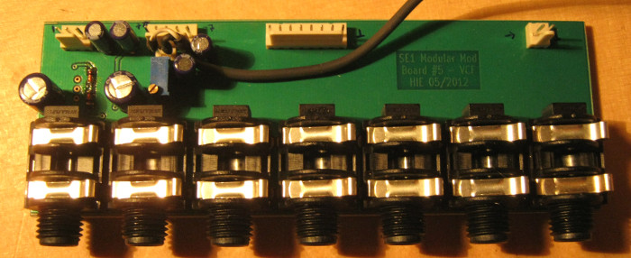
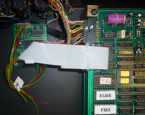
The later Elka Synthex models had a small MIDI interface built in, consisting of not more than a serial interface device (Motorola 6850), some glue logic and the obligatory photocoupler. The original boards are quite rare, and therefore rebuilds showed up over the years.
I’ve also designed a small board, using SMD components where possible for the ease of assembly and availability of components. Since the firmware used is still the unmodified original, the modern MIDI board suffers from the same problems as the original does – more messages than note on/off would probably screw up the small CPU of the Synthex.

Enough requests provided, a replacement CPU board allowing to MIDIfy the whole synthex (except the LFO section, because it’s strictly analogue) would be a possibe future products. So come on guys…

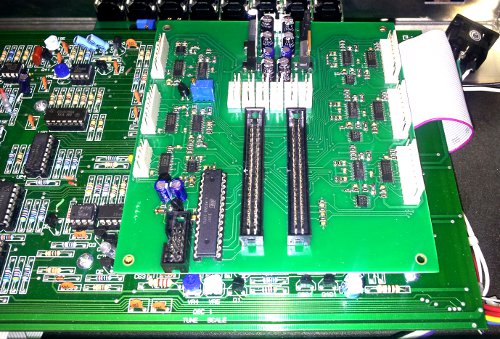
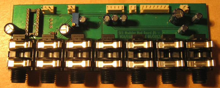
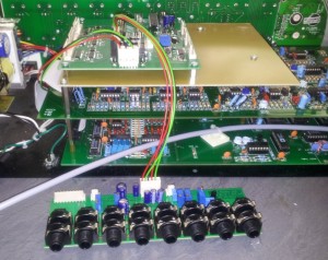
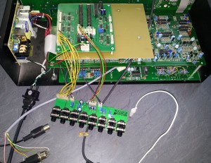
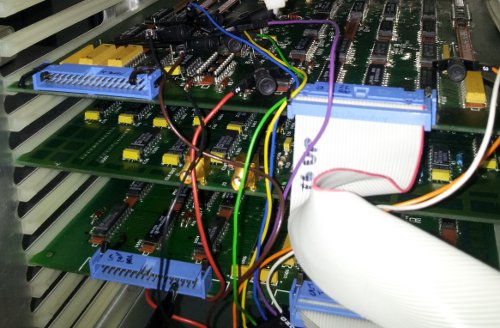
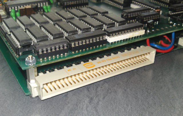
Oh sure, you want some tech stuff. Here it is, small enough to hide below the 24 wire strip cable:
MIDI board for the Elka Synthex

A Mega Cartridge for the DK Synergy

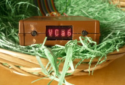
This Synergy ROM cartridge does not only behave like an easter egg, it also has some eggs inside

Megacartridge for the Synergy

Here the Mega Cartridge resembles the VCART6 cartridge, but that’s by far not the end. The initiator of this nice little project, Fabian Draeger, has just made a short video showing the prototype in action:

Right after inserting, the Mega Cartridge says hello and then immediately switches to the module last used.
In the video the VCART6 and the Wendy Carlos 1 are shown, but the memory inside is big enough to keep all official cartridges ever released. Depending on your interest, the Mega Cartridge will soon be available in quantities as fully built PCB. To compile your individual ROM, I would need proof of your ownership of the original cartridges for copyright reasons.

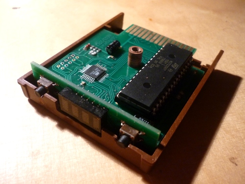
For the tech guys here's of course a photo of the inside

Mega Cartridge inside view

Old, new, white, blue

Something old – a PPG Wave 2.2 or 2.3,
something new – a 40×2 LCD,
something white – the LED backlight,
something blue – the background color

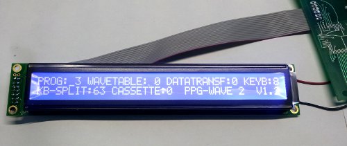
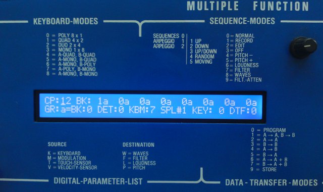
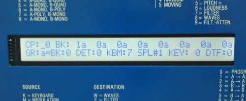
That’s the recipe for replacing a fading or just boring display in a PPG Wave, and here is how it looks like:

This is a drop-in replacement for all 2.2/2.3 that are already using the new HD44780-compatible display. It can be easily recognized – it is somwhat smaller than the old ones, revealing the metal frame on the front panel, and is mounted on some metal. Old 2.2 with the TAS82 require the on-board controller to be removed and some additional circuitry installed. The firmware is aware of both types.
Even refitting of Wave 2’s will be possible soon, I’m working on a firmware patch to allow the new type to be used with the Wave 2 as well.

And as a special gift, you get rid off that squealing noise of the inverter 🙂

To give you an impression how it would look like in ePaper-style – black on white – I’ve mounted  another display in the Wave. This type requires drilling some new holes, otherwise the LCD appears shifted to the right:

Wave 2 with backlit display…

A How-NOT-to-do-it guide

This Wave 2 owner decided that his PPG also requires a backlit display.
No problem so far. But the datasheet of the EL foil backlight stating that it need 200 to 250 volts AC obviously led to a very wrong decision:

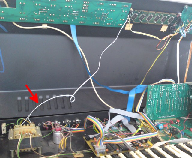
What we see here is an AWG28 2-wire cable ripped off from some flat cable, soldered to the primary lugs of the mains transformer -or, in other words – directly to the 230 VAC mains.
The other end is connected to the EL foil behind the LCD. Even the cheapest alarm clocks from the 70’s running EL illumination from the mains had at least a protective resistor in series.


PPG Waveterm B

Aside from some routine maintenance, this Waveterm B had a little devil sleeping inside for 25+ years now, showing that intuition and being insistent sometimes beat circuit analysis skills.
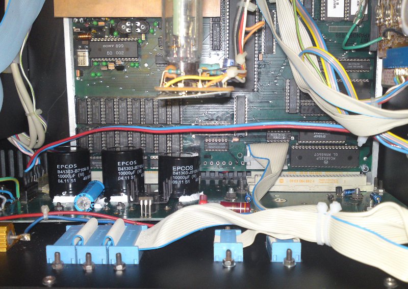
This is the inside of the Waveterm after completion:

What we don’t see:

  • complete rewiring of the mains supply to prevent short circuits or even electrocution of poor service personnel
  • new distance bolts and thermal grease for the voltage regulators
  • interconnections between the two computer boards soldered directly to get rid of the flaky connector
  • additional bolts to improve mechanical stability of the PCB sandwhich (see photo below)

What we do see:

  • new electrolytics in the power supply – yes, I dared to re-fit them the PCB, as they are much smaller than the orgininals and won’t get toasted by the DRAMs in full
  • EPROMs had their contents re-written from a known good Waveterm, as one had another checksum as a good dump of the same firmware version
  • All DRAMs at their places

Huh? Where else should they be if not in their sockets?
Hmmm.. let me think… lying in the dust, being stamped on by some heavy state elephants before real pain is being introduced to them?
Something else adequate to compensate for fooling me three hours? No understand?

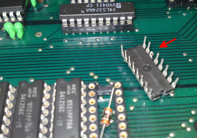
Look here:

Actually I don’t have much reason to complain. It worked for 25 years this way, much more one would expect from some modern high technology product. And it did work – sometimes, most of the time. But slight knocking would make the 68000 CPU part crash. After bending the DRAMs leg back everything is fine now for the next 25 years.

The two computer boards are stacked using some DIP40 sockets below the 6809 CPU and were only secured to each other on one side. To prevent this connection from becoming intermittent, I installed two additional bolts to hold them together on all 4 corners:


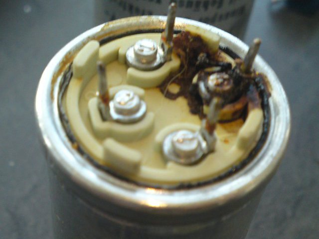
Finally I can show you a good reason to replace an electrolytic capacitor (no, this is not some kind of glue):


Rhodes Chroma – Troubleshooting the voice boards

When a Chroma sounds oddly or does not auto-tune reliably, 16 oscillator, filter and VCA circuits along with a handful of CMOS ICs are waiting for a check-up. Although the Chroma’s firmware has functions to support troubleshooting, several devices are hard to diagnose without the possibility to test the voice boards outside of the instrument.

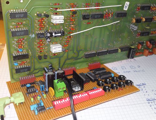
That’s why I built a simple test jig which allows to set all functions and parameters by means of DIP  switches and potentiometers.

With this set-up, verification of flawless function takes not much more than half an hour for all eight boards.
The board shown here has several faults – from two intermittent electrolytics over a broken 4556 CMOS 1of4-demux to a dead 4051, the latter two having been identified using the test jig.

Although this jig is rather primitive compared to my later design (Wave 2.2/2.3 test jig), it is still very helpful.

Wolfgang Palm : Der Kleine

(The Small / Tiny / Little One)

This blog is about the restoration of a very rare synthesizer: Der Kleine made by Wolfgang Palm, only three were built in the early 1970s.

It came to me together with the remainings of something which would eventually have been a case once upon a time. At  the moment, a new housing is being made from medium density fibre board (while chipboard is wood particles with some glue, MDF is just the opposite). Have a look at an early stage here:

In the mean time, the keyboard has been moved up about one centimeter, the spaces left and right from the keyboard are covered and a bottom cover is being cut and drilled these days.
After that, the case will be wrapped in some kind of artificial leather, just like the original.

[Update June 9: Der Kleine getting its new dress]

The red arrow i pointing to the only part taken from the old case for good karma: the wooden strip that supports the operating panel.
All potentiometers and switches will be replaced, a new power supply featuring a toroid transformer and for the first time compliance with the local electrical regulations will be built.
Several capacitors and resistors will be replaced, missing parts added, followed by a first test and calibration. Some more photos of the electronics will follow.

I’ve reverse engineered the circuit, a small service and usage manual will be available for download here soon. I’ll give some details on the circuit as well as on the functions and ranges of the knobs, so it would probably worth to read for musicians as well as for technicians.

The VCO of Der Kleine is somewhat different from the majority of other analog synths: it needs a linear-in-frequency control voltage, the slope will be around -118Hz/V calculated from circuit components.
No, no negative frequency, but negative CV 😉
To allow for external control, I’ll add a trigger input and for compatibility reasons a log-to-lin converter translating the usual V/oct control voltage into the linear scale needed by the oscillator.

Here’s a screen shot of some calculations done based on the values of resistor string on the keyboard, comparing the frequencies generated by Der Kleine to those of the actual note values (covering the range from F1 to C5)


Solina String Ensemble

These days a Mk.I String Ensemble made its way on my table.
While working perfectly without the ensemble effect, it showed some heavy noise and reduced volume in ensemble mode.

The noise turned out to be a defective TCA350Y BBD chip. While I’m waiting for the replacment part, I checked the other two delay circuits and found one showing no output at all. Fortunately only a transistor in the astable circuit driving the BBD’s clock inputs was intermittent, so all transistors of this type will now be replaced to prevent further trouble.

There were several types of this instruments available under different manufacturer labels – Solina, ARP and Eminent. The earlier models used TCA350Y BBDs while the latest had TDA1022s.

Consumer Information

(for the case your String Ensemble is missing one or more certain notes…)

At least three different top octave synthesizer chips (TOS) were used: M087, SAA1030 and TMS3616. All of those could be replaced by my universal replacement module RPLTOS or RPLTOS+.

Read more about this little board here http://huebnerie.de/index.php?article_id=14 (in German language)

Wave 2 DRS Adapter

The PPG WAVE2 DRS ADAPTER – demasked

First a short summary of the jacks and switches:
On the left we have 6 phone jacks labelled A to F, one named START/STOP
and a 5pin DIN connector for TAPE SYNC.

Three switches allow to enable a click sound (there’s a small speaker in the DRS box), one to choose between internal or external clock and another to select whether the clock outputs shall be 3 or 4 times the internal timebase.

The phone jacks on the bottom invite the user to feed either a contact-closure or positive voltage trigger signal, the third one labelled INPUT needs to be connected to  the trigger in jack on the Wave 2 – there’s no trigger input pin on the 14pin Amphenol connector, only an output!

Before I start with the description of the 5 right side jacks named CL.1 to CL.5 I’d like to tell all those people who can’t wait to hook this adapter to their Wave 2’s not to have too great expectations, or probably learn some 6809 assembly language.

No, let me start with the bad news instead of the clock outputs. The inputs A-F on the left are not connected within the box. The resistor pack which would close the circuit between the jacks and some port pins of the Wave 2’s VIA chip (which are, for those who really want to hack the firmware, the pins PA4..7 and PB0..1) is not fitted and has never been there.

Furthermore, no known firmware for the Wave 2 – and we know three different versions at the time of writing – has a single line of code that communicates with those port pins in any way.

Now let’s have a look at the circuitry that actually could work.
For understanding it is helpful to know that the Wave 2 has a programmable triple timer chip, a Motorola 6840. Timer #3 generates a clock signal that is normally fed to the clock input of Timer #1 through a 10k resistor. This allows to either tap the internal clock, or to override Timer #3’s output to force an external clock to become the clock source of Timer #1 and thereby control the clock for sequencer, arpeggiator and maybe other functions.

This mixed output/input is connected to the DRS box and directly available on the record out pins of the 5pin DIN jack for tape recorder connection. This allows to record the internal clock to a tape or cassette. In addition the clock signal is routed to two frequency dividers: one, dividing by 8, is selected by the clock switch in the x4 position. By using some advanced mathematics, I was able to calculate that the clock signal generated by Timer #3 is 32 times of … something.
For the x3 position of this switch, Wolfgang and his guys made quite some effort so the x3 clock scaling must have been very important. The clock signal is divided by a binary counter that resets itself when reaching a value of 11, but this would be a little bit too slow to reach 3 times the base clock (32/11 is less than 3, q.e.d.), so the counter is additionally reset whenever the counter of the by-8-divider reaches a value of 32. This way a mean frequency of 3 times something with some jitter is achieved.

Whatever the x3/x4 switch selects is buffered and shows up on the jack CL.1 at 5Vpp. CL.2 to CL.5 carry the clock from CL.1 consecutively divided by 2, 4, 8 and 16. That’s all. It’s up to your imagination what you could do with 3 or 4 times the internal sequencer clock. The CL.4 signal, namely 1/2 or 3/8 of the sequencer clock, makes the speaker click unless told not to do so by the CLICK switch.

If you have recorded some signal to a cassette, you would be able to send it back as the sequencer clock through the DRS box.
The playback pins of the DIN jack are followed by a detector (as simple as a CMOS Schmitt trigger) and a buffer which overrides the clock input of Timer #1 when the switch is set to EXTERNAL.

Finally there’s a START/STOP jack. It’ driven by an inverted version of the CA2 pin of the Wave 2’s VIA chip. When the sequencer is stopped, this pin goes high, disabling all the internal circuity of the DRS box – the counters of the frequency dividers are kept in reset state, and all outputs are forced low, including the tape recording output and the clock jacks.  The START/STOP output is low in this state. It goes high when CA2 becomes low, which is whenever the sequencer is started.

For those who still want to know everything about this little box, here’s the mapping between VIA pins and jacks:

A -> PB0
B -> PB4
C -> PA7
D -> PA4
E -> PA5
F -> PA6

WaveJig: a new helper for PPG Wave 2.2/2.3 voice board repair

Recently two PPG Wave 2.3 voice boards came in crying for help.
As I did not have a 2.3 in the workshop at that moment, I decided to build a test jig that allows to thoroughly check a voice board on the bench – actually much better than in the Wave, because it allows for well defined static levels that can be easily measured.

Here’s a photo for you:

On the left, you see a PPG voice board under test, my jig is plugged right onto it.

What it can do to help trouble shooting by now:
– generate a 20Hz triangle or 1kHz square wave through an arbitrary combination of voices A to D
– apply a control voltage between 0 and 3.5 volts to each VCA, VCF and resonance channel, independent from each other
– choose from any of the four possible time constants (0, 3, 11 and 14ms) for the VCA and VCF control voltages
– modulate the VCA and VCF control voltage for each voice with a 25Hz square wave to ease validation of those time constants

All functions are selected by short commands sent to the board via RS232, eventually by a nice little Tcl/Tk frontend… somewhen…

For now, it already helped me to identify 3 dead CD4066’s and one 74LS379 with a stuck low output – and also revealed a layout mistake on the voice board which prevents the 3 and 14ms time constant for voice D’s VCF from being selected, it will be either 0 or 14ms. Whether the 3 or 14ms setting is ever used is now a task for all 2.3 owners to find out 🙂 Theoretically, it could be audible if the VCF kicks in without a selected 3ms delay.